Part II: How significantly does the grain orientation affect inelastic damage accumulations in solder joints?
This article is the second part of a three-part series. Click here to read Part I.
 Due to the ever-increasing demand for higher performance in smaller portable electronic devices, advanced semiconductor packages have continuously decreased their solder interconnect size. The size can range from tens to hundreds of microns, containing only a few grains of SAC solder; in some cases, they contain only one or two grains. These microstructural variations occur even under the same assembly condition; Not only package-to-package variations but also joint-to-joint variations in the same package.

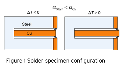
Grain-orientation-dependent inelastic strain evolutions of the SAC305 solder joint have been demonstrated successfully by the CALCE research team. A novel E-shaped symmetric configuration (Figure 1) was developed to apply a nearly pure shear loading condition to a single-grain SAC solder joint, produced by the CTE mismatch between the steel and copper legs.
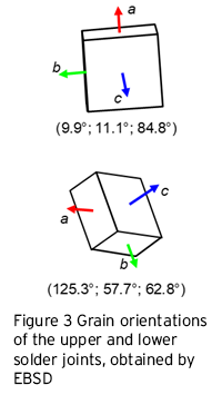
Moiré interferometry was then employed to measure the detailed in-situ deformations of the solder joints during a thermal cycle of -40 °C to 125 °C. Representative fringe patterns of the solder joints and adjacent areas captured during the 1st cycle are shown in Figure 2, where the contour interval is 417 nm. It is worth noting that despite the nearly symmetric global deformations, solder joints have significantly different permanent deformations after the cycle. Their grain orientations were quite different and so were their effective modulus in the loading direction (Figure 3).
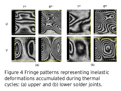
The permanent deformations accumulated after each cycle were recorded at 20 °C. The results obtained after completion of the 1st and 6th cycles are shown in Figure 4. Inelastic strain evolutions are observed.
The results were analyzed to provide a history of grain orientation-dependent inelastic strain evolutions. The inelastic shear strain accumulation per cycle was determined from the deformation fields, and the results are shown in Figure 5. The overall accumulated shear strain of the lower solder joint is smaller, indicating that the lower single-grain solder joint is more resistant to the shear loading compared to the upper solder joint due to its orientation. The results can be utilized effectively to calibrate and verify the anisotropic constitutive models developed for Sn-based Pb-free solder alloys. 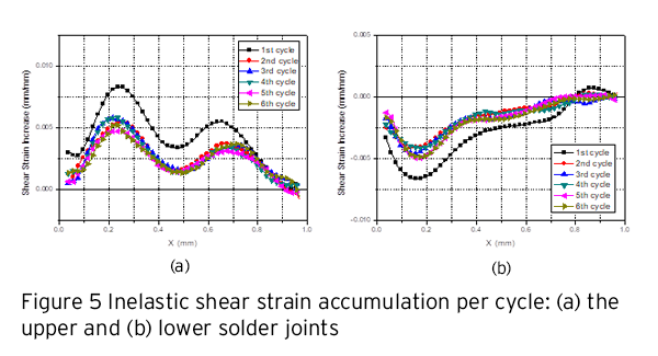
In the next article (Part III), a stochastic methodology to handle these microstructural variations for board-level reliability (BLR) will be introduced.
For more information about the anisotropy of solder joints, please contact Prof. Bongtae Han.
Top