Tin is one of the most common materials used in electronic products and systems. Tin is a highly abundant, low-cost, chemical element (Sn) that is chemically similar to both lead and germanium. It has a silvery appearance and is malleable. It oxidizes in air to form tin dioxide, but this oxide is self-limiting. Tin has a melting point of 231.9 °C, which is high enough for most application conditions, yet one that enables convenient manufacturing. Furthermore, tin has relatively good electrical and mechanical properties, especially when alloyed with lead. Thus, tin is commonly used in solders, as a surface finish for printed circuit boards, and as plating for connectors.
Tin is allotropic, meaning that it has different crystal structures under varying conditions of temperature and pressure. Tin has two allotropic forms. White β‑tin has a stable tetragonal crystal structure with a density of 7.31 g/cm3. Gray α‑tin, upon cooling below 13.2 °C, has a cubic structure and a density of 5.77 g/cm3. This α‑tin is also a semiconductor, not a metal. The expansion involves a change of crystal structure resulting in a ~27% volume increase. The α‑tin product, referred to as tin pest, is structurally weak, readily crumbles into powder, and causes most tin objects to crumble. Tin pest will usually nucleate at an edge, corner, or on a surface. Although tin pest can form at < 13.2 °C, most researchers believe that the kinetics are very sluggish at this temperature. There seems to be general agreement in the literature that the maximum rate of tin pest formation occurs at −30 °C to −40 °C.
A case study [1] of tin pest failure that occurred on plated electronical connectors exposed to low temperatures during storage confirmed the degradation of the connectors as a tin pest phenomenon. Several large tin-plated copper electrical connectors used in an electrical transit system in northeastern U.S. were analyzed. The connectors were located on the outside of the transit car and were used to conduct the electric supply from overhead cables to the transit car engine circuit. The connectors were coated with tin‑bismuth, containing 2% bismuth. Some of the coated connectors were put into service, whereas the remaining were boxed up and placed in a storage yard over the winter. Opening the boxes revealed a light-gray powder on the connectors.
Chemical analysis of the coating (unaffected and affected areas) indicated that some areas contained < 0.1% bismuth. The alloy was mainly Sn-10.85Cu, which is known to have a weak tin pest retardant. In this case, the plating procedure led to a bismuth-free plating being deposited on the connectors [36]. The tin, free of bismuth, was therefore susceptible to tin pest under low-temperature conditions (the outside temperature went below 13 °C).
Allotropic Transformation of Tin
The β → α transformation can be separated into two processes—nucleation and growth. The two processes occur at different rates, and nucleation is the critical event for tin pest formation. Nucleation is associated with long and uncertain incubation periods. Tin can spend anywhere from months to years in cold storage before developing observable signs of tin pest. Following nucleation, growth is relatively rapid, with 100% transformation to α‑tin observed to occur in as little as 30 days [21].
As shown by Nogita et al. [22], the deterioration of the sample was due to a combination of the 27% volume expansion and the embrittlement of the material. Further chemical differences between β‑tin and α‑tin include a change in electron configuration from s2p2 to sp3, a reduction in coordination number from 6 to 4, and a change from metallic bonding to covalent. The semiconducting properties of α‑tin are a result of the covalent character of atomic bonding, which causes a change in electronic band structure. A separation of valence and conduction bands produces an energy gap of 0.08 eV.
Xu [23] reported new findings discovered in his research on gray α‑tin. Xu found that α‑tin exhibits a novel electronic phase when its crystal structure is strained, putting it in a rare new class of 3D materials called topological Dirac semimetals (TDSs) The bulk electrons in TDSs behave as massless Dirac fermions in all three dimensions, which leads to the possibility of novel physical behaviors, including ultrahigh carrier mobility, giant linear magnetoresistance, chiral anomaly, and novel quantum oscillations. TDSs can reveal many interesting topological phases under controlled conditions. They can also undergo phase transitions and become a topological insulator (TI), a Weyl semimetal, or a topological superconductor.
Xu strained the crystalline structure of the material by growing α‑tin samples in layers on InSb substrate. InSb has a slightly different lattice constant which puts strain on the α‑tin structure either by compression or tension. Furthermore, this discovery showed that α‑tin under a compressive strain is not an insulator, as had been thought. It turns out to be a Dirac semimetal. Based on Xu's calculations, α‑tin becomes a TI only under tensile strain conditions. His findings can open up many new research directions and help researchers understand and use α‑tin electronic properties.
RoHS and Some Exemptions
On 1 July 2006, a new European Union directive, the Restriction of Hazardous Substances (RoHS), took effect. This directive restricts the use of six hazardous materials, including lead, in the manufacture of various types of electronic and electrical equipment. Therefore, new lead-free solders had to be developed, the most common being tin‑copper, tin‑silver, and tin‑silver‑copper. All three alloys have similar solderability properties as the lead‑tin solders, however, they do not have the same inherent resistance to tin pest. Alternatives to tin have raised product reliability concerns over the possibility of tin pest formation in solder joints of low-temperature application devices [2]. Transformation of β → α tin in electrical devices implies the potential for disintegration of solder joints, loss of electrical connectivity, and complete failure of the device.
The uncertainty as to whether tin pest would be an issue led to applications to the RoHS for special lead-free exemptions such as the one by the European Coordination Committee of the Radiological, Electro-medical and Healthcare IT Industry [3]. The application, titled “Application for granting new exemption: Lead in solder for electrical circuitry that is used at temperature below −20 °C,” recommended exemptions for certain medical devices for which operating temperatures could reach as low as −269 °C.
According to Article 5(1)(a) of the RoHS, exemptions are granted when applications can demonstrate that compliance with RoHS materials bans will result in any one of three conditions, among which is the condition that the reliability of substitutes is not ensured [4]. Publications that demonstrate a greater susceptibility of lead-free solders to tin pest, such as the one by Plumbridge [5], are cited in the application mentioned above to support the claim that there are no suitable alternatives to tin‑lead solders and that continued use of tin‑lead solders is required to ensure the reliability of certain low-temperature application devices. Exemption 26 in Annex IV of the RoHS was thus approved for the use of lead in various components of electronic packaging intended for applications below −20 °C. Although the exemption was approved, the underlying technical justification for the exemption is incomplete because it used only a portion of the available literature on tin pest in lead-free solders. The studies that were not included highlight a disparity between the formation of tin pest in bulk samples of lead-free alloys and in actual leadfree solder joints. In order to make a more complete assessment of the issue of tin pest in lead-free electronics, the entire body of available evidence must be considered. The evidence for tin pest resistance by lead-free alloys in solder joints is strong. Although traditional tin‑lead solders have been observed to resist tin pest for greater periods of time in studies of bulk samples, studies that have investigated lead-free alloys in electronic packaging demonstrate a resistance of solder joints to formation of tin pest that could be used to present a counter argument to lead-free exemptions.
Tin pest in tin alloys
Over the past several decades, tin‑lead solders have been preferred for interconnecting and packaging electronic components. However, since 2006, with the passage of the RoHS directive, the electronics industry has been undergoing a lead-free revolution. The result has been the transition away from traditional tin‑lead solders to lead-free alternatives containing a substantial percentage of tin. The transition of the electronics industry toward lead-free solders has once again shifted the discussion to the risks of tin pest, primarily when the solders are alloyed with lead-free materials. Pure tin is generally not accepted in the electronics industry due to another failure mechanism known as tin whiskers. Nevertheless, some studies of bulk alloy samples suggest that lead-free alloys exhibit greater susceptibility to tin pest than traditional tin‑lead solders. Clearly, this is not acceptable for electronic systems that must be reliable below 13.2 °C. Yet, although tin pest has been reported to occur in the laboratory, there are no examples of tin pest ever occurring in the field. In fact, the electronics industry has generally operated under the premise that tin pest will not occur if tin is alloyed.
Most of the available research on tin pest in lead-free solders is performed on bulk samples of varying shapes and sizes. Despite the increased susceptibility of lead-free solders observed in bulk samples [2,4,7–9], it has been suggested that tin pest formation in solder joints will be opposed by the physical properties of the solder joint itself [2,6,10,30-35]. The size and geometry of the solder joint, as well as the constraint of the adjacent substrate and components in an electronic assembly, are factors that are not assessed in studies of bulk samples, but have been implicated in the resistance of solder joints to tin pest. Solder joints consist of a very thin layer of solder between the substrate (PCB) and the joining component [2]. Consumer trends and product miniaturization will, in time, decrease the solder layer into what is essentially a plane. In a study by Matvienko and Sidelnikov [9], sample geometry was observed to directly affect the formation of tin pest in samples of pure tin. The dependence of growth rate on sample thickness was observed by measuring the spread of tin pest in samples of variable thickness following seeding with α‑tin. The growth rate decreased with decreasing sample thickness. The effect of sample thickness on formation of tin pest was attributed to an increase in crosssectional dislocation density with decreasing sample thickness. Increasing the dislocation density produces an increase in the internal stress, which acts to oppose recovery processes and inhibit tin pest formation.
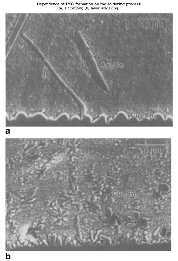
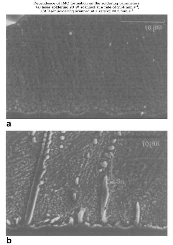
The small size of the solder joint implies greater significance for dispersion strengthening produced by the formation of an intermetallic compound (IMC) [11]. In addition to the IMC that forms as a result of the alloy composition, intermetallic phases are produced as a result of the manufacturing processes [6,11]. Dissolution of metals from the adjacent components or substrate metallization occurs during the solder reflow process. The small size of the solder joints means that partial substrate dissolution can significantly change the liquid composition, introducing new elements into the alloy or shifting the concentrations of existing elements away from the eutectic composition [6,12]. Eutectic Sn-Ag solders joined to copper or copper alloy pads have been observed to incorporate the copper and develop Cu-Sn IMC along the copper/solder interface [12]. These intermetallic phases form as either dendrites or interface layers. The degree of copper dissolution and IMC formation is dependent upon both the soldering process and the process parameters. Laser soldering, for instance, has been shown to increase the total amount of Cu6Sn5 in the solder joint relative to infrared (IR) reflow (bottom left figure) [13]. Increasing the beam power and beam scan rate was also shown to increase the formation of copper IMCs (bottom right figure) [13]. The under-bump metallization (UBM) often contains other elements such as Ni and Au, which will similarly affect the solder composition and increase the amount and variety of intermetallic phases. The increased volume fraction of IMC in this case will further strengthen the material and increase resistance to tin pest.
 Literature studies on tin pest in tin-based solders
Peng [6] performed a limited investigation on the potential of tin pest formation in lead-free solder joints. Two mobile phone boards, one with joints of QFN (quad flat no leads) package mounted with Sn-3.8Ag-0.7Cu solder paste and the other with traditional Sn-36Pb-2Ag solder paste reflowed on Ni/Au-plated ball grid array (BGA) pads were exposed to low temperatures to determine if tin pest would form over the 5.5-year observational period. After the study, neither phone board had developed signs of tin pest. Tin pest resistance was attributed to a matrix-strengthening effect from a fast cooling rate and dissolution of UBM during reflow. It was suggested that the reduced size of the solder balls promoted a high rate of cooling and resulted in smaller tin grain sizes and fine intermetallic crystals, which strengthened the solder joint and increased tin pest resistance. A similar mechanism was proposed for the dissolution of UBM metals during reflow, where Cu, Ni, and Au increased the volume fraction of IMCs in the solder, further strengthening the joint and increasing resistance.
Earlier studies assessed the potential for tin pest formation in largemodel solder joints [2]. Three solder alloys were tested: pure tin, highpurity tin‑lead (Sn-Pb), and a commercial solder alloy. Solders were joined with copper and then seeded with α‑tin. The study found that tin pest formed on all but the commercial solder, but tin pest resistance was attributed to impurities rather than the physical characteristics of the joint. In actual solder joints, the proportion of free surface is considerably less than that of the model. Given the propensity for tin pest to form along free surfaces or edges where constraint is at a minimum, the large size of the solder joint does not accurately model the conditions in actual solder joints. Additionally, by seeding the joints with α‑tin, any inhibitive effect that the solder geometry or assembly might have, independent of size, on preventing nucleation is not assessed.
As mentioned earlier, studies observing growth characteristics by seeding with α‑tin are of limited importance for solder joints, as it would suggest tin pest has already nucleated. Understanding the criteria for nucleation is of interest for assessing the viability of lead-free alternatives and electronic reliability. The proportion of available free surface for tin pest to form on should be significantly less for the actual solder joints than the model [2]. Although the surface area to volume ratio is increased by miniaturization, the small size of the joint and contact with the substrate and adjoined component reduces the amount of free surface for tin pest to form on. The effects of both high pressure and physical constraint on preventing tin pest have been demonstrated in earlier studies. Contact surfaces help to prevent the formation of tin pest by restricting the volume expansion associated with the transformation from β → α‑tin. The effect of surface constraint is like that of the material bulk resisting nucleation at the interior of the sample. Plumbridge [2] suggested that resistance to the volume expansion is related to the deformation/fracture characteristics of the material in contact. Tin pest can only form under these circumstances if its formation energy overcomes the deformation strain energy of the material.
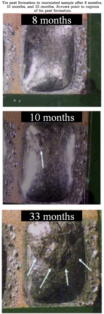
In a study by Hillman [14], test electronic assemblies were created with pure tin solder alloys to see if tin pest could be induced in solder joints composed of abnormally high concentrations of tin. Conventional industry surface mount soldering processes were used to simulate the conditions of a “real world” printed wiring assembly. The final composition of the solder paste was 89 mass% pure tin with the addition of 11 mass% flux. The assemblies were divided among three treatments. Group 1 (n =2) was subjected to thermal shock testing between −40 °C and +40 °C temperature extremes. The transition from one extreme to the other extreme took 60 s, with dwell periods of 20 min.
Assemblies were inspected for tin pest formation every 500 thermal cycles over a total of 3000 thermal cycles. Group 2 (n = 5) was subjected to a constant −40 °C, and assemblies were inspected for tin pest formation once per week. Group 3 (n =2) received identical treatment to group 2 with the additional inoculation of select solder joints with α‑tin crystals. Groups 2 and 3 were kept in cold storage for 33 months. Groups 1 and 2 remained free of tin pest over the entire observational period, while tin pest was observed to occur in the inoculated samples of group 3 after 8–10 months' exposure (the right figure). By using solders of unusually high tin content, this study represents an extreme case of lead-free solders in low-temperature electronic applications. It is expected that the performance of common lead-free alternatives will be equal to or better than the tested solders under identical conditions. The reaction of the high‑tin-content solders to both thermal shock and constant low-temperature exposure for 33 months demonstrates an increased resistance of lead-free alloys in solder joints relative to similar lead-free alloys in bulk samples. Kariya et al. [7] showed that even inoculated solder joints exhibited tin pest resistance comparable to that of non-inoculated samples of Sn-0.5Cu, which were observed to develop tin pest after ~7 months.
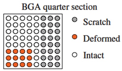
Fig. I Defects on solder balls of BGA components.
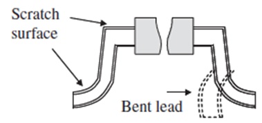
Fig. II Defects on leads of QFP components.
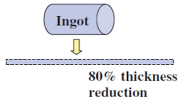
Fig. III Ingot samples of bulk solder cold-rolled to 80% thickness reduction.
Fig. IV Boards with pads plated with InSn finish.
Fig. V Comparison of XRD spectrum for SnAgCu (SAC) ingot sample aged at −30 °C and non-aged.
Studies on the surface finishes of electronic components
In addition to solder material, electronic equipment manufacturers have traditionally used tin‑lead as a surface finish to maintain the solderability of metal surfaces and provide protection against corrosion. With the movement of the electronics industry away from traditional tin‑lead alloys, part manufacturers have selected pure‑tin or high‑tin content lead-free alloys that are compatible with lead-free solders to replace tin‑lead as a surface finish. Similar to concerns over the reliability of lead-free alloys in soldered interconnects, the elimination of lead has raised concern for the reliability of pure tin, or high‑tin-content lead-free alloys used in the surface finish of terminals in packaged electronic devices and printed wiring boards. Common alloys for packaged devices include tin, tin‑copper, and tin‑bismuth. For printed wiring board finishes, immersion tin and lead-free hot air solder leveling (Pb-free HASL) are used. Lead-free HASL may use a tin‑silver‑copper or tin‑copper alloy. Lead is known to mitigate some of the deleterious phenomena caused by tin, such as tin whisker formation and tin pest formation. While tin whiskers have received considerable attention and test standards have been developed regarding them, the focus on tin pest has been limited in these applications [15–17].
The Center for Advanced Life Cycle Engineering (CALCE) at the University of Maryland had investigated (unpublished research) the occurrence of tin pest in lead-free alloys for a variety of sample types including electronic components and pad finishes on PCBs, with bulk lead-free ingot samples as comparators. Electronic components included BGAs with Sn-3.0Ag-0.5Cu solder balls, and QFPs (quad flat packages) with a termination finish plating of Sn, Sn-0.7Cu, and Sn2.0Bi. Bulk solder samples included Sn-3.5Ag, Sn-0.7Cu, and Sn-3.0Ag-0.5Cu, and board pads were plated with immersion tin. To initiate tin pest formation, a variety of surface defects were introduced in the electronic component samples. Solder balls on the BGA componentswere either deformed by 100 μm or scratched by knife-edge (Fig. I). Tin-finished terminal lead wires on the QFP were either bent or scratched by knife-edge on the shoulder and foot areas of the leads (Fig. II). Bulk samples were cold-rolled to 80% thickness reduction in a similar attempt to promote tin pest formation (Fig. III). No defects were introduced on the In-Sn-plated board pads (Fig. IV). Samples were exposed to either −30 °C or −80 °C and were removed for inspection at ~3 month intervals.
All samples resisted the formation of tin pest for 29 months of exposure at −30 °C and 20 months at −80 °C. This was confirmed by X-ray diffraction (XRD) analysis where the diamond cubic crystal structure of α‑tin was not identified for any of the samples. A comparison of XRD spectra taken for two SnAgCu (SAC) bulk ingot samples, one aged at −30 °C and the other non-aged, shows no difference between diffraction patterns for both samples (Fig. V). Table I shows the diffraction patterns for white and gray tin and can be used to verify the absence of α‑tin in both the aged and non-aged samples shown in Fig. V. Scanning electron microscopy (SEM) was also used to inspect the formation of α‑tin. SEM inspection of the lead wires did not find any abnormal formation indicating α‑tin.
Table I Diffraction patterns of the white and gray tin.
|
White tin (α)
|
Gray tin (β)
|
|
D (Å)
|
Intensity
|
2θ
|
D (Å)
|
Intensity
|
2θ
|
|
2.915
|
100
|
30.64
|
3.751
|
100
|
23.7
|
|
2.793
|
90
|
32
|
2.294
|
83
|
39.24
|
|
2.062
|
34
|
43.86
|
1.956
|
53
|
46.38
|
|
2.017
|
74
|
44.9
|
|
Following the initial exposures, samples were refrigerated for an additional 6 years under less controlled temperatures below 13 °C. Following the additional refrigeration, total exposure time of the samples was ~8.75 years and ~7.5 years for the −30 °C and −80 °C groups, respectively. Subsequent examination failed to identify any observable signs after the additional exposure. The resistance to tin pest formation by the cold-rolled bulk samples of Sn-0.5Cu contrasts with observations made by previous studies. Mechanical deformation, in this research by CALCE, was intended to promote tin pest formation, however, the cold-rolled Sn-0.5Cu samples resisted tin pest for greater periods of time relative to cold-rolled samples from the study by Di Maio and Hunt [18], and also resisted tin pest for greater periods of time relative to as-cast bulk samples from the study by Kariya et al. [7]. The resistance to tin pest by SAC solders in the BGA components over the exposure periods for both temperatures is generally consistent with observations of bulk tensile samples of these alloys in research conducted by Plumbridge [8] and Matvienko and Sidelnikov [9]. Similar to the results discussed in Hillman's research [14], Plumbridge and Matvienko and Sidelnikov reported that the resistance to tin pest of the pure tin, coating the board pads, is significantly greater than that of pure tin in bulk samples from other studies.
The results of CALCE's research demonstrate the ability of lead-free alloys to resist tin pest in multiple uses in electronic packaging at least as well as, and in some cases better than, similar alloys in bulk samples from other studies. Additionally, the resistance to tin pest of the electronic components over the observation period following the introduction of surface defects suggests that characteristics of the solder joint may inhibit the effects of mechanical deformation and other factors known to promote tin pest in bulk samples. Finally, the results indicate that tin pest formation is unlikely to occur on electronic assemblies with lead-free tin.
Nucleation mechanisms
The discovery of artificial nucleation was key to the early study of the growth phase of the β →α transformation. Although it was well understood that seeding tin would accelerate the transformation by eliminating the long and uncertain periods of nucleation, the process of artificial nucleation was not extensively studied, and instead was one of many tools available to researchers for use in the investigation of other factors, such as composition, and their effects on the rate of tin pest formation. Despite its significant use, the criteria for nucleation and the underlying mechanisms were not well understood. In a study by Styrkas [10], new and existing experimental data were compiled to examine the key features of nucleation and identify the processes underlying the formation of α‑tin.
Styrkas [10] investigated the role of metastable structures in the induction of nucleation. Nucleation had previously been observed to be accelerated by the interaction between seeds and β‑tin. Of interest was the ability for seeds to facilitate nucleation even in instances of indirect contact. It was unclear how, for instance, an inert substance that had previously been in contact with a seed could initiate formation of α‑tin after the seeds had been removed. It was proposed that nucleation could be due to the condensation of atmospheric water vapor forming metastable cubic ice on the surface of seeds. The dependence of various nucleation mechanisms on the formation of metastable cubic ice was examined by observing the potential for nucleation to occur in tin samples exposed to conditions intended to prevent the condensation of atmospheric water vapor.
Nucleation was first initiated in the presence of atmospheric water vapor to establish a baseline for the various mechanisms of nucleation including initiation by contact with seeds, by proximity to seeds, by contact with inert substances previously in contact with seeds, as well as by spontaneous nucleation. In the control experiments, nucleation of tin by the same mechanisms was investigated for samples prepared either in evacuated tubes or desiccation chambers, or following treatment with acetone, ethanol, or glycerol. Treatment with acetone, ethanol, or glycerol was done to seeds for contact with seeds, and proximity to seed mechanisms, while treatment was applied to the glass (inert substance) for contact with inert substances previously in contact with seed mechanisms. This was intended to prevent nucleation by dissolving the epitaxial cubic ice and breaking down its structure. Storage of samples in the evacuated tube and desiccation chamber was intended to prevent nucleation by removing the atmospheric water vapor. It was expected that if nucleation were seeded by structural ice, then nucleation would be inhibited under those conditions that prevented its formation. For each mechanism, nucleation did not occur under any of the control conditions. These results support the proposed role for metastable cubic ice in seeding the formation of α‑tin in cases of nucleation by proximity to seeds and by contact with inert substances previously in contact with seeds. The results further demonstrated the dependence of nucleation by contact with seeds and spontaneous nucleation on the formation of metastable cubic ice.
Sn-O in the seeding nucleation
The study [10] similarly investigated the role of metastable structures in seeding nucleation by the memory effect. Nucleation has been observed to occur more rapidly in tin samples that have previously formed α‑tin, but have been heated to cause the transformation of α‑tin to β‑tin. Even if α‑tin is completely transformed, samples do not return to the initial density of the untransformed 100% β‑tin composition. Chemical analysis found samples to contain up to 0.03 w/o oxygen. It was suggested that the deviation in density and the trace oxygen content could be explained by the oxidation of α‑tin to a metastable oxide (SnO) when exposed to air during the heating process. With a similar crystal structure to α‑tin and the ability to persist in a metastable phase beyond the α→ β transformation, the accelerated nucleation of these samples following subsequent cooling was attributed to the epitaxial growth of Sn-O on the α‑tin.
Skwarek et al. [24] investigated the role of Sn-O in seeding nucleation by observing nucleation under conditions intended to prevent the formation of Sn-O. Samples were prepared with pressed-in seeds of α‑tin and sealed in evacuated tubes. Once all samples were found to undergo the β →α phase transformation, they were then heated to room temperature to initiate the reverse transformation back to β‑tin. As samples were heated, half of the tubes were opened to the air immediately while the other half were kept sealed for 2 h to ensure the transformation was completed in the absence of atmospheric oxygen. It was expected that if nucleation were seeded by Sn-O, then formation of α‑tin would be inhibited in samples that were kept sealed and prevented from oxidizing. Only those samples immediately exposed to the air were observed to undergo the β → α transformation following subsequent cooling. Nucleation did not occur in those samples that remained sealed in the tubes during the α→ β transformation. It was suggested that nucleation did not occur in sealed samples because there was no oxygen to oxidize the α‑tin to Sn-O.
These results support the proposed role for Sn-O in seeding the formation of α‑tin in the memory effect. Additionally, the use of conventional seeding methods to produce the initial transformation to α‑tin while samples were sealed in evacuated tubes provides further support for the dependence of nucleation by contact with seeds on the formation of metastable cubic ice. Initiating the transformation to α‑tin in the absence of both atmospheric water vapor and oxygen demonstrated that the interaction between thermodynamically stable seeds and the β lattice is sufficient to induce nucleation, given the interaction occurs in close molecular contact. Considering nucleation by contact with seeds does not occur unless atmospheric water is present, these results suggest a need for cubic ice to grow in an epitaxial direction on the seed and establish a contact with the β lattice that the seed alone is unable to produce without mechanical pressing.
Studies on the nucleation incubation
Skwarek et al. [24] used the conventional seeded growth method to investigate the influence of inoculator type on the induction of α‑tin growth. Although artificial nucleation had been shown to accelerate the transformation to α‑tin, the relative effectiveness of different seeds was not yet understood. In addition to investigations of inoculator type, the effect of mechanical and chemical treatment of samples, in conjunction with inoculation, on the initiation of α‑tin was also investigated. It was suggested that inoculation alone was limited in how fast it could produce the formation of α‑tin, and that incubation periods could be further shortened to < 24 h by combining inoculation with additional mechanisms known to facilitate nucleation. We assume that there should be some effect of mechanical treatment because the deformation of samples by cold re-education generally leads to reduced periods of incubation and accelerated growth of α‑tin. This effect of mechanical treatment is attributed to the increase of internal compressive stress providing an additional driving force for the transformation from β to α‑tin.
Treatment of the β‑tin surface with HCl was shown by Styrkas [10] to accelerate artificial nucleation. HCl treatment is intended to facilitate nucleation by the partial, or whole, dissolution of the SnO2 oxide layer, which forms on the surface of β‑tin. The oxide layer is said to obstruct the interaction of the seed and β‑tin, and thus, the removal of this layer by treatment with HCl accelerates the transformation by improving contact between the seed and the β lattice. Bulk samples (n= 30) of Sn-1Cu (Cu purity of 99.9 wt%) were cast in roller-shaped ingots (1.0 cm diameter and 0.7 cm height) and drilled on the upper surface to make a hole of 2 mm depth and 1.5 mm diameter. Samples were then dipped in HCl and divided into three groups (n= 10) where they were inoculated with α‑tin, Cd-Te, or In-Sb. The concentration of the α-phase in the α‑tin powder was 30%, while In-Sb and Cd-Te were 99.99% pure. After filling the drilled holes with powdered inoculant, the samples were mechanically deformed. A force of 30 KN was applied to samples in the direction perpendicular to the inoculated surface, producing cold thickness reduction of 70%. The three groups were divided once more (n =5) for exposure to either −18 °C or −30 °C. Samples were observed for signs of nucleation on intervals that did not exceed 24 h. All samples were observed to form α‑tin in< 24 h. Samples inoculated with α‑tin and stored at −30 °C underwent short incubation periods and exhibited high rates of transformation. In-Sb produced the greatest transformation rates at −18 °C. The inoculator with the greatest influence on growth rate varied between the two temperatures, suggesting the β → α transformation is dependent on temperature in addition to inoculator type. The induction of nucleation in< 24 h is a significant increase over transformation rates from previous studies conducted by Skwarek et al. [24]. The improvement demonstrates the effectiveness of combining multiple sample treatments to accelerate the β → α transformation. Additionally, this study succeeded in developing a reproducible method for rapid nucleation that can be used by other studies to improve the speed and reliability of transformation kinetics.
Transformation Kinetics
Nogita et al. [22] took advantage of modern analytical techniques to investigate the kinetics of the β →α transformation, which have traditionally been difficult to study due to the relatively slow rate at which it occurs and the long incubation periods that precede it. In this study, variable-temperature synchrotron powder XRD (PXRD) was used to investigate the isothermal growth characteristics of the β → α transformation in seeded high-purity (99.99% Sn) powdered samples of tin. This method represents a significant improvement over other methods such as differential scanning calorimetry (DSC), dilatometry, electrical resistance measurement, and microstructural observation. The transformation can be studied more precisely, and the exposure temperature can be controlled while phase analysis is performed by XRD.
By cooling the sample and holding it at a specific temperature, while analyzing the phase composition, the transformation from β to α‑tin was tracked over time for a range of temperatures. Quantitative Rietveld refinement was conducted to calculate the weight fraction of the α and β phases from XRD results, which were used to quantify the volume fraction of α and β phases from XRD results and construct isothermal transformation vs. time curves for each holding temperature. Transformation kinetics were then expressed by the Johnson–Mehl–Avrami–Kolmogorov (JMAK) equation.
(t) = 1 – e – ktn (1)
Eq. 1 is a function of fraction transformed X(t), and K and n are constants. The equation was reworked, and the transformation vs. time curves were expressed by Eq. 2.
ln [1 (1–X)−1] = n ln(t) + ln(K) (2)
The transformation turns the isothermal transformation vs. time curves into linear approximations with gradient n and intercept ln(K), referred to as the JMAK plot. The Avrami exponent for all curves in this study was 3, which describes transformation where nuclei are present at the beginning of the transformation and kinetics are governed by the 3-dimensional growth of nuclei. The best-fit JMAK constants were used to construct TTT (time-transformation-temperature) curves for the β → α transformation.
The samples consisted of seeded high-purity (99.99% Sn) powdered samples of α‑tin. The α‑tin samples for PXRD were created by storing 99.99% pure tin at −45 °C for 180 days where samples underwent β → α transformation, disintegrating into powder. The α‑tin samples were then loaded for analysis and heated to 50 °C to cause the transformation back into β‑tin. Data was collected for 10 min at 50 °C to characterize the β-phase. Samples were then cooled to −10, −20, −35, −45, −60, −85, and −100 °C at a rate of 6 °C/min followed by 10 min of isothermal data collection at the respective temperature for up to 30 measurements. In all samples, α‑tin peaks were either absent, or at low intensity starting out, but grew in intensity with time and as the transformation proceeded. Transformation to α‑tin occurred most rapidly in samples cooled to −45 °C. Transformation to α‑tin did not occur at all in samples cooled to −10 °C and −20 °C. Additionally, −10 °C and −20 °C samples were the only samples to completely transform to β‑tin during 10 min of annealing at 50 °C. All other samples had α‑tin peaks of varying intensity at the first measurement, suggesting the α→ β transformation did not go to completion at these temperatures and α‑tin remained in these samples to seed growth upon subsequent cooling. Two-phase Rietveld analysis was used to plot the isothermal transformation curves. The curves have sigmoidal shape and demonstrate that the β →α transformation did not go to completion. JMAK plots for the isothermal transformation curves were well approximated by linear curves with R2 values of 0.933. Avrami exponents of 3 are consistent with these samples as most contained smaller amounts of pre-existing α‑tin from incomplete α →β transformation during annealing. As well, it is likely that the α‑tin spreads in three dimensions in powdered samples in accordance with n = 3. The constants from the JMAK equation were used to plot the TTT curve. The curve has a C shape, with the shortest incubation period and most rapid transformation occurring at ~−45 °C as predicted from the isothermal XRD data. Rates are slowed at temperatures above and below −45 °C, indicative of a balance between thermodynamic driving force and transformation kinetics. The TTT curve can be used as a baseline for examining the effects of composition on β →α transformation [9].
Impurities effects on the β → α transformation
In a study by Zeng et al. [25] the β → α transformation was shown to be affected by impurities. The effect of impurities on tin pest formation is related to the solubility of the inclusion. Matvienko and Sidelnikov [9] reported that Ge promotes tin pest (similar crystal structure to α‑tin) and inhibits growth of tin pest relative to pure tin. The study investigated the role of 1 wt% Pb, Cu, Ge, and Si on the isothermal kinetics of the β →α transformation. It is unclear from this study how Ge and Si would affect the transformation kinetics due to the similarity of their crystal structures to α‑tin.
Zeng et al. [25] used the same sample preparation as the study by Nogita et al. [22] except 1 wt% of 99.99% purity Pb, Cu, Gu, or Si was added to powdered α‑tin prior to annealing. One sample of pure tin without inclusions was prepared for comparison. All samples were annealed at 50 °C for 10 min before cooling at a rate of 6 °C/min to a temperature of −45 °C, at which point isothermal data was collected over 10-min intervals for up to 38 measurements (rather than vary the temperature as in a previous study, the samples were all run at the same temperature, but with different composition, to determine the effect of element additions).
Two samples of pure tin were prepared: one was annealed for 10 min like the rest, the other for 20 min to determine any effect of additional time for the α →β transformation on the kinetics of β → α transformation upon subsequent cooling. XRD data for different annealing times of tin show that transformation is slowed with longer annealing. The time until detection of α‑tin as well as time until reaching the maximum transformation rate are both shorter for the 10-min tin sample. Zeng et al. [25] used the same methods as Nogita et al. [22] for making the isothermal transformation curves. Transformation was more rapid in tin annealed for 10 min and progressed further as well. The transformation kinetics significantly slowed for all samples with elemental additions. The shape of the element addition curves was not sigmoidal like the rest, suggesting that the transformation mechanism was altered from 3-D growth of preexisting nuclei. 1 wt% Pb demonstrated the slowest transformation, supporting the relationship between solubility of element and effectiveness at inhibiting tin pest. Ge and Si kinetics were greater than Pb and Cu, but still significantly slower than tin. The abnormal shape of the isothermal transformation curve for element additions is translated to JMAK. The transformation kinetics of pure tin annealed for 10 min are nearly perfectly described by the linear relationship of Eq. 2 with an Avrami exponent of 2.96. This represents a modified JMAK model where an impingement factor c is introduced to better suit the isothermal transformation kinetics exhibited by the tin alloys. In summary, Pb and Cu demonstrated the greatest capacity to prevent the transformation, while Ge and Si, although their kinetics were higher, were still significantly slower than pure tin despite having similar crystal structures to α‑tin.
Transformation can be separated into two distinct processes—nucleation and growth [2]. Nucleation is described as the formation of a diamond cubic unit cell. In this case, nucleation entails the generation of a particle of α‑tin from the atomic rearrangement of the β lattice. Nucleation is favored at temperatures below 13.2 °C where the thermodynamic driving force increases as exposure temperature decreases. Following nucleation, growth occurs by the progression of the β →α transformation and by the migration of the β →α interface into the untransformed region of β‑tin [5]. Migration of the β → α interface is described as a balance between the accumulation of lattice stresses and relaxation of the stresses by recovery processes. Lattice expansion generates stresses associated with structural and volume misfit between the α and β phases as atoms move and bonds are bent out of position. The build-up of stress in the crystal lattice acts to oppose the progression of the β → α transformation by inhibiting the atomic rearrangement of the crystal structure. The transformation from β‑tin to α‑tin will proceed by relaxation of stresses in zones of plastic deformation in the β-matrix ahead of the migrating interface. Recovery processes accomplish stress relaxation through the creation and movement, or annihilation, of dislocations in the β‑tin lattice. The nucleation of tin pest and the rate at which tin pest grows are thus determined by mechanical characteristics of the β-matrix and the rate of stress relaxation. Factors that contribute to lattice strength and reduce the mobility of lattice defects will serve to inhibit tin pest formation [1,5].
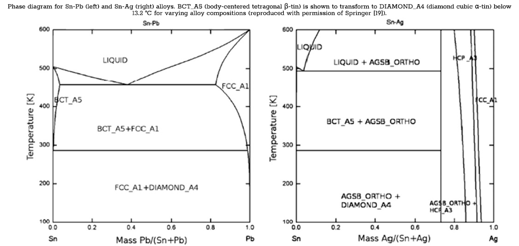
The stability of the β‑tin phase down to temperatures of 13.2 °C is demonstrated in phase diagrams of common alloys of tin with varying concentrations of bismuth, lead, or silver [7,20]. According to the phase diagrams, the transformation from β‑tin to α‑tin will occur in the small corner of the β‑tin phase region for compositionally pure tin below the 13.2 °C transformation temperature. The restriction of the α‑tin phase to such a small region of the phase diagram demonstrates the effectiveness of smaller amounts of bismuth in preventing the formation of tin pest. Bismuth content at these levels can be commonly found even in commercially pure tin as trace impurities [2,7]. The phase diagrams for Sn-Pb and Sn-Ag in the following figure further represent the ability of α‑tin to form in tin alloys [7]. The difference in the size of the α‑tin phase region between the three diagrams demonstrates the variability in the relative effect of different elements in stabilizing the β phase and preventing the β → α transformation. In these diagrams, the horizontal phase boundary at ~283 K (13 °C) shows that the transformation from β → α tin will occur below the transformation temperature for compositions up to ~99 mass% Pb and ~72 mass% Ag. Rather than stop the transformation outright, inclusions affect the rates at which the different transformation processes occur, thereby delaying nucleation and slowing the growth rate. The relative effect on the time until nucleation and on the growth rate varies from one element to the next and in relation to inclusion concentration.
Independent of composition and impurity effects, nucleation and growth proceed at different rates [2]. The kinetics of the β →α transformation is, in general, slow and is hindered by long and uncertain periods of incubation. Following nucleation, the spread or growth of α‑tin proceeds relatively quickly. Samples in low-temperature exposure commonly remain unchanged for periods of a few months to several years before nucleation occurs and the first visible signs of tin pest emerge. For pure tin, the subsequent transformation can take only days and entails the disintegration of the sample into a powder of α‑tin. The two processes are variable and appear to be controlled by several factors.
It has been suggested [21] that all nucleation mechanisms depend on the interaction of the β lattice with any one of several known “nucleates” or “seeds”. Seeds are described as substances that have crystal structures isomorphic to α‑tin, with similar lattice parameters. The following table presents a list of common seeds and their crystalline properties. The interaction of tin with the “foreign” crystal structure of seeds produces strain on the β lattice, which provides the force necessary to initiate the rearrangement of the β‑tin atoms into the diamond cubic structure [21]. This means seeds act as nucleation sites, with the formation of α‑tin occurring directly on the surface of the seed. There is a distinction among common seeds between those that are thermodynamically stable (α‑tin, Cd-Te, In-Sb) and those that form a metastable phase (cubic ice, Sn-O). Although the effect of their interaction on the β lattice is the same, the ways in which the two types of seeds can establish contact with the β lattice, and the conditions under which that contact is made, differ between the two types of seeds. Interaction between a seed and the β lattice is required to occur on the molecular scale to produce the strain on the β lattice that initiates the formation of α‑tin [21]. For thermodynamically stable seeds, contact with tin is established when seeds are intentionally introduced for purposes of research, or contact can occur by incidental introduction as contaminants from external sources. In either case, physical contact between a seed and tin is not always sufficient to produce an interaction at the molecular level due to the oxidation of the β‑tin surface. Exposure to atmospheric oxygen results in the formation of a SnO2 surface layer, which blocks seeded growth and prevents seeds from making the necessary molecular-scale contact with the β lattice. In conventional seeded growth, this is overcome by mechanically pressing the seed into the tin to penetrate the surface oxidation layer. If molecular-scale contact is not established by mechanical pressing, nucleation requires the formation of non-equilibrium structures such as metastable ice. The condensation of atmospheric water vapor onto seeds creates an epitaxial layer of structured water with a cubic lattice of metastable ice. When the seed is not in close molecular contact with the β lattice, either contacting the tin surface or even near it, without physical contact, epitaxial cubic ice crystals are able to reach the β lattice through micropores in the oxide film and act as seeds to facilitate nucleation. Structural ice plays a similar role in the nucleation of α‑tin from contact with inert substances. When an inert substance, such as glass, meets a seed, the epitaxial cubic ice that has grown on the seed can persist on the glass surface after the removal of the seed. This metastable ice can seed nucleation upon contact with tin.
Crystal data for β‑tin, α‑tin, and common seeds
|
Substance
|
System
|
Lattice parameters, Å
|
Coordination number
|
Interatomic distance, Å
|
|
β-Sn
|
Tetragonal
|
a = 5.83,
c = 3.18
|
6 (4+2)
|
3.03 (4), 3.18 (2)
|
|
α-Sn
|
Cubic
|
a = 6.489
|
4
|
2.79
|
|
InSb
|
Cubic
|
a = 6.478
|
4
|
2.78
|
|
CdTe
|
Cubic
|
a = 6.41
|
4
|
32.77
|
|
Metastable ice
|
Cubic
|
a = 6.36
|
4
|
2.76
|
|
SnO
|
Tetragonal
|
a = 3.8,
c = 4.84
|
4
|
2.26
|
The formation of non-equilibrium structures has been implicated in another nucleation mechanism involving tin that has experienced thermal cycling through the allotropic transformation temperature in the presence of air. When tin that has previously undergone the β → α transformation is heated above 13.2 °C, it will begin the reverse α→ β transformation. If the α→ β transformation does not go to completion before subsequent cooling, the nucleated state is maintained and further transformation into α‑tin occurs more rapidly. Even if the transformation eventually goes to completion, α‑tin is oxidized during the heating process, resulting in the epitaxial growth of a tin oxide (SnO) directly onto the α‑tin. SnO is structurally like α‑tin, and its metastability can persist beyond the conversion of α‑tin back to β‑tin. This is referred to as the “memory effect” where metastable SnO acts as a “memory carrier” during subsequent cooling to seed the nucleation of α‑tin. Unlike the previously described processes, contact between seed and β lattice in the memory effect requires specific conditions where some degree of thermal cycling has allowed for the prior formation of α‑tin. With the condition of prior α‑tin formation satisfied, the epitaxial growth of a metastable structure (SnO) off the α‑tin seed is similar to the epitaxial growth of cubic ice, except in this case, there are no obstacles to the interaction of SnO and the β lattice because the β lattice is formed in direct contact with β‑tin [21]. Each of the mechanisms described so far is in some way the result of, or facilitated by, the introduction of thermodynamically stable seeds. These mechanisms are referred to as “artificial nucleation”. Theyare facilitated by pre-existing seeds and do not reflect a mechanism for nucleation, which would occur in tin alone without the fulfillment of some given pre-condition. Spontaneous nucleation still requires the interaction of a seed and the β lattice to initiate the formation of α‑tin. Metastable ice also acts as the seed; however, growth of the metastable phase occurs directly on the surface of the tin.
Each of the different mechanisms of artificial nucleation can accelerate nucleation and reduce the incubation period by several orders of magnitude, relative to spontaneous nucleation. It is likely that the long and uncertain incubation periods associated with spontaneous nucleation are due in part to their dependence on the formation of metastable cubic ice directly on the tin surface. Epitaxial growth of the metastable structures in artificial nucleation occurs more easily because of the similarity of crystal structures between the metastable seed and the existing seed on which it forms. In spontaneous nucleation, the growth of metastable cubic ice directly on the tin surface is energetically less favorable and depends on fluctuations in conditions such as pressure, temperature, and humidity.
Previous tin pest research on various tin-based solders with different elements inclusion
Much of the foundational work on tin pest occurred from 1930 to 1960 [2,7]. Studies investigated the effects of factors such as composition, impurity level, strain, and microstructure on the occurrence and growth rate of tin pest. Researchers took advantage of the ability to accelerate nucleation and reduce or eliminate the long and uncertain incubation periods by artificial nucleation. Thus, most of the early studies focused on the growth of tin pest and understanding the influence of these factors on the transformation.
Kariya et al. [7] investigated the effect of alloy inclusions on the growth rate of tin pest by observing the length of time for formation of a visible wart following inoculation with 0.1 mg α‑tin. The study included 8 different binary alloys. The results show that growth proceeded most rapidly in the pure tin, developing within 2 h after inoculation. Alloys of copper were marginally effective at slowing the growth rate, with visible warting observed 4–7 h after inoculation. Pb, Bi, and Sb alloys slowed the rate of growth of tin pest from hours to days. Three different alloys of Pb were tested with increasing mass% compositions (0.024, 0.48, and 50 mass% Pb). The results suggest that the growth rate slows in relation to the amount of Pb, with the amount of time until wart formation increasing from 12 to 29 to 190 days, respectively. 0.1 mass% Sb slowed the time for formation to 14 h, while 0.5 mass% Sb remained free of visible warting beyond the 5.5-year observational period. 0.3 mass% Bi slowed the growth rate to 330 days after inoculation. The rapid formation of a visible wart in a period of 2 h suggests that pure tin is most susceptible to tin pest. The delayed formation time observed in all alloys demonstrates a role for alloy inclusions in inhibiting tin pest growth by slowing the transformation rate. The effectiveness of the different alloys at inhibiting growth is related to the solubility of the alloying element in tin. The more soluble elements such as Pb, Sb, and Bi slowed the rate of growth to a greater degree than the relatively less soluble Cu.
Additional studies [2] of composition further investigated the effect of solubility of alloy inclusions on tin pest resistance by performing tests on a range of elements with different solubility. Low-solubility inclusions such as Zn, Al, Mg, and Mn were observed to accelerate growth. Cu, Fe, and Ni inclusions did not produce a significant effect on the growth of tin pest. Reports on the effect of Cu were inconsistent, however, with later work providing evidence of a role for Cu in promoting tin pest. The inconsistency could potentially be explained by differences in the elements present in either sample between the two studies. This study reported that the influence of an alloying element could change, either inhibiting or promoting tin pest growth depending on the presence of other atoms. Further evidence for the effect of soluble inclusions came from a study investigating the effect of extremely low levels of high-solubility inclusions on the growth of tin pest. It was discovered that as little as 0.0035 mass% Bi was effective at inhibiting the growth of tin pest.
Temperature effects on the growth of tin pest
Investigations of temperature on the transformation from β → α tin found that the growth rate of tin pest will increase with decreasing temperature [2]. Observations of growth in inoculated samples found the relationship held until reaching a maximum linear growth rate of 0.006 mm/day at −40 °C. Beyond this temperature, the relationship flipped and growth rates declined with further decreases in temperature. Growth rates at −18 °C were measured at about one-third the maximum rate at −40 °C.
The transformation from β →α can be inhibited by factors that oppose the associated volume expansion [2]. Tin pest resistance has been shown to increase in relation to increased external pressure. By increasing the external pressure, lower temperature is required to increase the thermodynamic driving force and overcome the constraint. The temperature of formation is thus reduced by 50 °C per Kbar.
Variability is exhibited in the number of samples that develop tin pest. Only one of four samples developed tin pest after exposure for 6 months to −73 °C, the rest remained free of tin pest for over 4 years [2]. The same study determined that tin pest could be prevented for up to 4 years following inoculation in cold-worked pure samples of Sn, Sn-40Pb, and Sn-50Pb by the addition of 0.1 mass% Bi or Sb. Investigations of nucleation in non-inoculated samples of Sn, with small additions of Pb, Bi, or Sb, identified the critical amounts of solute for each element needed to prevent nucleation for 14 months at −73 °C (0.18, 0.047, and 0.27 mass%, respectively).
Impurities effects on the growth of tin pest
An alternate study on nucleation investigated the role of impurities on incubation time and nucleation rates in 21 varieties of commercially pure tin with 0.002 to 0.246 mass% impurities [2]. In only one variety did most samples develop tin pest. Samples were observed to develop tin pest between 5 and 114 months, demonstrating the variability in the incubation period. Nucleation was observed to occur in 4 other varieties, but< 20% of samples developed tin pest in these groups. Tin pest was not observed to occur in any samples of the remaining 16 varieties. It was concluded that the resistance of the 16 varieties that did not develop tin pest in any samples could be attributed to the presence of impurities.
Mechanical treatment effects on the growth of tin pest
Studies that investigated the effect of mechanical treatment on tin pest formation returned inconsistent results [2]. One study reported that cold rolling prevented the formation of tin pest in 11 out of 12 samples for periods> 10 years. Samples of identical composition were observed to develop tin pest in 22 out of 24 without cold rolling, suggesting that mechanical deformation promotes tin pest resistance. These results conflict with an alternate study on mechanical treatment, which observed higher tin pest formation in cold-worked samples. Further support for mechanical treatment promoting tin pest came from a study investigating the effect of tensile pre-strain on tin pest growth in tin-coated steel. Tensile pre-strain promoted tin pest formation, suggesting a general trend of mechanical treatment promoting tin pest formation.
These studies characterized many of the factors that control the transformation from β →α tin. Temperature, mechanical treatment, composition on the level of both global and trace inclusions, surface constraint, and the relative solubility of inclusions were all identified as playing some role in determining the susceptibility of tin or its alloys to tin pest formation. A precise understanding of how these factors affected susceptibility was, however, still unclear. This was due largely to the level of inconsistency between these early studies such as in the reported effects of Cu inclusions on growth rate and of mechanical treatment. Experimental procedures and observational techniques often varied from one study to the next, producing inconsistent or sometimes conflicting results. These variations in methods meant that reported findings were thus specific to the conditions of that experiment, making comparisons between studies difficult or altogether impossible [2].
Recent research on the tin pest within the most common lead-free solders
The recent shift in the electronics industry to lead-free soldering has brought a renewed research interest in the issue of tin pest. The binary and ternary alloys of tin with Ag and Cu (Sn-0.5Cu, Sn-3.5Ag, and Sn-3.8Ag-0.7Cu) are among the most common lead-free alternatives. Considering the propensity for tin pest to form in pure tin [7], the dilute compositions of common lead-free alternatives have directed research focus to the potential for these alloys to develop tin pest (the following figure). Although the growth phase of the β → α transformation has been extensively studied, significant knowledge gaps remain on the criteria for nucleation of tin pest [2]. Thus, recent studies have centered on understanding the different factors affecting the incubation periods and rates of nucleation for common lead-free alloys.
Studies on the incubation period of tin-based lead-free solders and alloys
An observational study by Plumbridge [2,8] and Gourlay et al. [26] investigated incubation periods and nucleation rates of lead-free alloys by comparison to traditional tin‑lead solder. Bulk samples of 5 different tin alloys (Sn-Pb, Sn-Cu, Sn-Ag, Sn-Ag-Cu, and Sn-Zn-Bi) were exposed to subcritical temperatures for periods of> 10 years. Samples were monitored for observable signs of tin pest formation. Alloys of Ag and Cu were reported to be the most susceptible, with Sn-0.5Cu being the first to exhibit signs of tin pest formation. Surface discoloration was observed in Sn-0.5Cu within just a few months, progressing to surface eruptions, warts, surface cracking, and eventually total disintegration of the sample. The Sn-Pb comparator was the only one to remain free of tin pest up to 10 years. The first signs of tin pest were not observed in Sn-Pb until the 12th year of exposure. The Sn-Zn-Bi alloys were reported to be the only samples to have remained free of tin pest at the end of the study, but it was noted their exposure had been limited to a period of up to 6 years. An assessment of all samples showed there was significant variability as to whether, or how quickly, tin pest would form for each of the alloys. Samples from all alloys except Sn-Zn-Bi were observed to develop tin pest at different rates under identical conditions. For example, Ag and Cu alloys (Sn-3.5Ag, Sn-3.8Ag-0.7Cu, and Sn-3.0Ag-0.5Cu) were observed to have developed tin pest within a broad window of ~4–8 years. Additionally, in those alloys that did form tin pest, transformation was rarely observed to occur in 100% of the samples. So, while tin pest disintegrated some samples into powders of α‑tin, other samples of identical composition and exposure remained free of tin pest. From the results on the occurrence of tin pest in the 5 different alloys, it was concluded that most, if not all, tin-based alloys will develop tin pest when exposed to temperatures below the allotropic transformation for tin. Although Sn-Zn-Bi resisted tin pest for the period of the study, it was speculated that with additional time, tin pest would be observed in these alloys as well. The shorter incubation period observed in the binary and ternary alloys of Ag and Cu is evidence of an increased susceptibility to tin pest relative to the traditional Sn-Pb eutectic alloy. The general variability in the incubation period and nucleation rates supports the earlier findings by Bornemann [27] andsuggests a role for something other than bulk composition in the nucleation process.
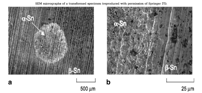
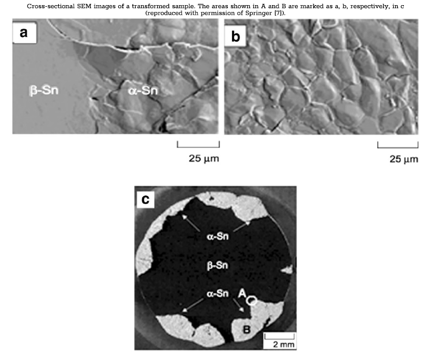
In a study by Kariya et al. [7], the incubation period and nucleation rates of one alloy, Sn-0.5Cu, were observed in greater detail. Samples were observed to have incubation periods of around 1 year, with some samples developing tin pest in as little as 7 months. These results are consistent with the results from Plumbridge [2], where Sn-Cu alloys exhibited relatively high susceptibility with the shortest incubation periods. Observations were carried on beyond the incubation period to detail the growth characteristics of tin pest. In the sample that developed tin pest after 7 months, 40% of the surface was covered after 1.5 years, spreading to 70% by 1.8 years. The relatively rapid spread of tin pest following the 7-month incubation period emphasizes the difference in the rate at which nucleation and growth occur. SEM images were taken of localized areas of α‑tin, as well as the transformation boundary between β- and α‑tin regions. The disturbed or rough surface pattern is associated with the growth of nucleated α‑tin grains and the localized volume expansion. The cross-sectional images show that growth originates from the surface of the material (the following figure). The transformation will progress along the surface of the material and gradually penetrate the interior. These observations are supported in the study by Peng [6], where nucleation was observed to occur on the edge of the plate before propagating into the bulk of the sample. In general, nucleation in the interior of a sample is unlikely due to the constraint of the surrounding material on the associated volume expansion. Growth occurs most often along a free surface or edge where constraint is at a minimum. This agrees with the earlier findings on the effect of pressure inhibiting the growth of tin pest. The surrounding bulk material acts similarly to increased external pressure to resist the formation of α‑tin.
Peng [6] investigated of the effect of composition on the occurrence of tin pest in rolled sheet samples of pure tin, Sn-Pb, and three common lead-free alloys (Sn-3.5Ag, Sn-0.7Cu, and Sn-3.4Ag-0.8Cu). Samples were exposed to low temperatures for a total of 5.5 years after which, only samples of pure tin had undergone nucleation. These results demonstrate the greater susceptibility of pure tin to the formation of tin pest, but also highlight the types of inconsistencies commonly observed in tin pest studies. In the studies by Kariya et al. [7] and Plumbridge [2], samples of Sn-Cu had reasonably similar incubation periods where both were observed to develop tin pest after around 1 year of exposure, sometimes sooner. Small variations are expected according to experimental evidence from the two studies, however, resisting tin pest for 5.5 years, as was observed in the study by Peng, represents a significant deviation from the general trend of 1 year. This scenario is complicated because some samples from Kariya et al. [7] and Plumbridge [2] never developed tin pest at all. It is difficult to say, one way or the other, whether 5.5 years is unusually long when there is so much variation in the literature. In the context of the bigger picture and understanding nucleation criteria for reliability of solder joints, these results suggest that the issue of tin pest cannot be understood in terms of global composition alone, and that additional factors must be accounted for to develop a more complete understanding of tin pest.
The inconsistency in the proportion of samples that undergo nucleation is well documented both in earlier studies of pure tin, and in the studies described above on lead-free alloys [2,5–8]. It was demonstrated in earlier work that small amounts of inclusions or impurities could be effective at extending the nucleation period and increasing the resistance of a sample to tin pest. In a study by Leodolter-Dworak et al. [17], variances in the composition of trace elements in two samples were investigated as a potential cause for inconsistency in rates of nucleation. Two Sn-0.5Cu samples with identical composition and treatment history were contributed from the study by Kariya et al. [7]. In one sample, the transformation to tin pest had disintegrated the sample into powder, whereas the other sample had remained entirely free of tin pest. The concentrations of 23 elements were analyzed using ICP-OES. The analysis identified statistically significant differences in 9 of the 23 elements. For every element for which significant differences were found, the higher concentration was always found in the tin-pest-free sample. Among the elements present in higher concentration were Pb, Bi, and Sb—high-solubility elements that have been shown to be effective at inhibiting tin pest formation and extending the incubation period. These results support earlier work by demonstrating, in greater detail, the role for trace amounts of solute or impurities in conferring tin pest resistance [2]. Additionally, these results support earlier findings on the effect of solubility of inclusions in promoting tin pest resistance. Based on the findings of this study [2], it is possible that differences in the amount of trace impurities are responsible for the inconsistency observed in rates of nucleation. Another important note to make about these findings is the implications for use of commercialpurity solder vs. high-purity solder. Considering the levels of impurities reported in commercial-purity solders from an earlier study (0.002 to 0.246 mass% in some cases) [2], it would suggest that in addition to being economically favorable, the use of commercial solders with these levels of impurity is in fact beneficial in preventing the formation of tin pest.
Microstructures of tin pest
Microstructural characteristics are commonly used to assess the susceptibility of lead-free alloys to tin pest. Common Ag- and Cu-based lead-free solders differ from the traditional tin‑lead solders in that they are much more dilute, with at least 95 mass% tin, owing to the relatively low solubility of Cu and Ag in tin [2,19,20]. The high solubility of Pb in Sn creates a microstructure composed of significant proportions of a tin‑lead solid solution. In lead-free alloys, the high tin content, coupled with low Ag and Cu solute concentrations, produces a distinctly different microstructure characterized by large regions of high-purity tin phases (~0.1 mass% Ag and 0.006 mass% Cu) with intermetallic crystals of Sn-Ag and Sn-Cu distributed homogenously throughout [5,7,24]. Given the propensity of tin pest to form in pure tin, where rates of both nucleation and growth are observed to be highest, the large regions of β‑tin have been suggested as one cause for the increased tin pest susceptibility of lead-free alloys relative to traditional tin‑lead [2,8].
The significance of the two different microstructures is in the strengthening effect on the β-matrix and the mechanism by which stress relaxation is opposed. The formation of a solid solution between Sn and Pb solute atoms produces a solid solution-strengthening effect [2]. The dissolution of Pb solute atoms helps to retain stresses in the matrix by creating localized lattice distortions, which interact with and oppose the migration of dislocations [9]. This effect increases with solute concentration. The formation of intermetallic crystals by the precipitation of excess solute in lead-free solders works in a different manner to oppose the relaxation of stresses by dispersion, or precipitation strengthening [2,6]. Instead of an interaction between dislocations and individual atoms, intermetallic crystals prevent dislocation migration by pinning grain boundaries and increasing the elastic modulus of the alloy. This effect is proportional to the amount of solute and thus the number of IMCs. The strengthening effect of IMCs in leadfree solders is, however, less than that of solid solution strengthening observed in tin‑lead solders due to the relatively low volume fraction of IMCs.
There is disagreement in the literature over the effect of IMCs on promoting or inhibiting tin pest. In contrast to the role of IMCs in dispersion strengthening of the β‑tin matrix, IMCs have been described as the unfavorable result of the low solubility of inclusions such as Ag and Cu [2]. The accumulation of excess solute and the precipitation of IMCs have been cited as producing instability, ultimately increasing tin pest susceptibility by serving as sites of nucleation for α‑tin. However, the effectiveness of IMCs in promoting or inhibiting tin pest is a matter of perspective. The matrix-strengthening effect of IMCs may not be as strong as other more soluble inclusions, such as Pb, but in comparison to pure tin, any amount of β-matrix strengthening caused by IMCs will create a relative increase in tin pest resistance, as reported in the literature.
Cooling rate effects
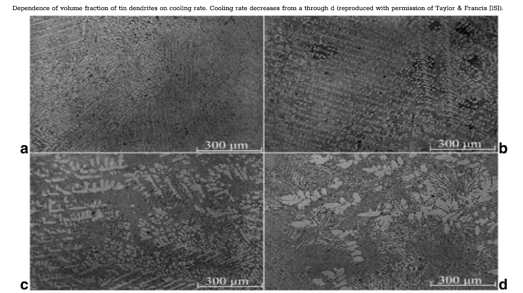
The significance of microstructure in the strengthening effect on the β-matrix, and more generally, on tin pest resistance, implies that factors such as cooling rate will influence tin pest resistance as well. Cooling rate has been shown to affect the relative amounts and the distribution of different phases produced during the solidification process [12,25]. Higher cooling rates are of particular interest for lead-free solders because they occur during manufacturing due to the small size of solder joints [6,12,15]. During the cooling process, in both the binary and ternary lead-free alloys, tin regions form as dendrites [25]. As previously mentioned, these regions have compositions that deviate from the global composition and are more similar to that of pure tin (< 0.04% Ag in Sn-3.5Ag solders and< 0.01 wt% Ag/<0.006 wt% Cu in Sn-3.8Ag-0.7Cu). Following the dendrite formation, a eutectic structure forms in the inter-dendritic regions. In binary solders, this binary eutectic structure is composed of tin and an intermetallic phase of the alloying element (Sn-Ag3Sn or Sn-Cu6Sn5). In ternary alloys, a ternary eutectic structure is formed composed of tin and both the Ag and Cu intermetallic phases (Sn-Ag3Sn-Cu6Sn5). Snugovsky et al. [15] investigated observing the effect of cooling rate on the microstructure in eutectic SAC solders. Samples were cooled at different rates over the range commonly used in reflow soldering (0.2 K s−1–10 K s−1). Higher cooling rates were observed to increase the volume fraction of β‑tin dendrites (the following figure) This observation is supported by measurements, where volume fractions of tin increased from 25% to 40% at rates of 2 K s−1 and 10 K s−1, respectively. The low Ag and Cu content in the tin regions meant that these elements became concentrated in the interdendritic regions. This concentration of Ag and Cu in the inter-dendritic region produced an increase in the volume fraction of the two intermetallic phases in the eutectic-like structure. The effect of higher cooling rates is thus a redistribution of tin from the eutectic structure to the tin dendrite phase composed entirely of β‑tin. This would suggest that relatively less tin forms in the eutectic structure with intermetallic compounds to provide precipitation strengthening. Thus, it would be expected that the microstructure produced by higher cooling rates would be more susceptible to tin pest formation.
The effect of cooling rate on the length of incubation period and rates of nucleation was investigated as part of a larger study by Plumbridge, described above [2,8,9]. During preparation, samples of 5 different alloys were cooled at one of three different rates, water quenching 20 °C s−1, air cooling 0.2 °C s−1, and furnace cooling 0.02 °C s−1, and stored at low temperatures for periods > 10 years. The results did not conclusively demonstrate a role for cooling rate in affecting nucleation processes. General trends can be teased out of the data by narrowing the scope of the observations, for instance, tin‑lead alloys were observed to develop tin pest on exclusively water-quenched samples when exposed to −18 °C. This would support the idea that microstructures formed by rapid solidification promote tin pest, but the relationship does not hold for all alloys such as tin‑copper, where furnace and air-cooled samples demonstrate greater tin pest susceptibility.
Temperature Effects on Metallurgical Processes
The effect of temperature on both the duration of the incubation period and the growth rate is complex, involving a balance between the thermodynamic driving force of the β → α transformation and transformation kinetics [2,7,8]. As temperature decreases, tin pest formation is favored as the thermodynamic driving force is increased. At lower temperatures, however, lattice strength is increased and transformation processes are kinetically inhibited. This relationship has been demonstrated for pure tin both in the earlier studies described above and in an alternate study by Matvienko and Sidelnikov [9], where tin pest growth rates in samples of pure tin were measured over a range of temperatures from −50 °C to 0 °C. Growth rate exhibited a nearly symmetrical trend, increasing steadily from −50 °C, peaking sharply at ~−23 °C, then falling back down to below the initial measured rate at 0 °C (the following left figure). Although the measured values of maximum growth rate, and the temperature at which it occurred, do not match the earlier findings, the relationship between temperature and the two processes producing a single maximum is consistent between the two studies. The same relationship was demonstrated in a tin alloy of Sn-Ge (the following right figure). In this figure, the original results for pure tin are plotted for comparison. Alloying with Ge is shown to inhibit the rate of growth while still maintaining the same general trend in response to varying temperature.
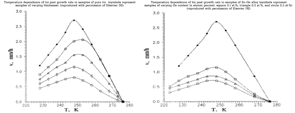
The effect of temperature on nucleation rates is not as clear as the effect on growth demonstrated in the study by Matvienko and Sidelnikov [9]. Among the studies that have observed the length of incubation and the rates of nucleation at varying temperatures, the results have been largely inconsistent [2,8,9]. Peng [6] exposed samples of pure tin, Sn-Pb, and three common lead-free alloys (Sn-3.5Ag, Sn-0.7Cu, and Sn-3.4Ag-0.8Cu) to a series of three temperatures for varying lengths of time. Temperature and exposure period went from −196 °C for 50 h, to −40 °C for 4 years to −17 °C for 1.5 years. Growth was only observed in samples of pure tin during the 1.5-year period at −17 °C. The absence of tin pest formation at the lower temperatures was attributed to low atomic mobility preventing the transformation into α‑tin. The effect of temperature on incubation period and nucleation rates was also observed in the study by Plumbridge [2,5,8]. Samples of each of the five different alloys were kept at constant temperatures of either −40 °C or −18 °C for the duration of the study. In binary Sn-Cu and ternary Sn-Ag-Cu samples, pest formation was greatest at −18 °C while tin‑lead samples transformed to the greatest extent at −40 °C. The absence of a distinct trend in the effect of temperature on tin pest susceptibility in alloys suggests that the effect of temperature on nucleation is potentially alloy-specific, with the balance between thermodynamic driving force and transformation kinetics depending on the composition of the solder.
Temperature effects on tin pest formation
The stepwise increase in temperature and the abbreviated exposure periods administered in the study by Peng [6] limit its effectiveness in furthering the understanding of the influence of temperature on the development of tin pest. Drawing conclusions about the effect of an individual temperature on the formation of tin past following prior exposure to lower temperature conditions assumes that there is no accumulated effect of low-temperature exposure on the development of tin pest. In other words, the development of tin pest at any given temperature is assumed to be independent of any previous exposure to different temperatures; a nucleation event is essentially binary, where the criteria are either met or not met; and there is no intermediate stage or progression to the initial development of α‑tin that could be affected by previous exposure to different temperatures. Additionally, the absence of tin pest in all but the pure tin samples after the 5.5-year period is insufficient basis for drawing conclusions about the relative effect of different temperatures in tin alloys. Considering the length of incubation periods observed in the study by Plumbridge [2], much longer observational periods are required to assess the effect of any factor on the formation of tin pest.
Temperature has also been implicated in the formation of tin pest through the process of aging under non-equilibrium conditions [2,6,20]. The rapid cooling rates experienced by solder joints in the solidification process cause the formation of non-equilibrium phases [6,12,19] and the build-up of residual stresses in the microstructure of alloys. For common Ag and Cu lead-free alloys, this often entails the formation of phases that are super-saturated with low-solubility alloying elements. At lower temperatures, these phases are unstable, and thus microstructural changes, such as the precipitation of intermetallics, are made to accommodate the instability and assume more energetically favorable conformations. Given that IMCs serve to increase the strength of the material through precipitation or dispersion strengthening, it is possible that aging may serve to increase tin pest resistance in common lead-free alloys. The microstructural changes associated with aging also act to relieve the residual stresses that form during solidification [2,6]. In this manner, aging has been suggested to promote tin pest formation by facilitating the recovery processes and plastic deformation involved in the transformation from β → α tin.
Influence of aging
In the context of tin alloys and the effects of aging on tin pest formation, the distinction between aging at temperatures above and below the 13.2 °C transformation temperature must be made. Although both aging processes constitute non-equilibrium conditions, aging at temperatures above 13.2 °C is regarded in the literature as a pretreatment administered prior to low-temperature exposure. Although the range of non-equilibrium temperatures over which aging processes occur may represent a continuum, aging at, for instance, room temperature is considered distinct in most studies from any microstructural changes that may occur during low-temperature exposure.
Plumbridge [2] investigated the effect of pre-aging on the development of tin pest in the study of incubation period and nucleation rates discussed above. Samples were aged for 100 h at temperatures between 75 °C and 130 °C prior to low-temperature exposure. Relative rates of nucleation were observed for aged samples. These temperatures represent relatively high homologous temperatures for these alloys so it was expected that microstructural changes would consume the internal stresses that oppose the β → α transformation, thus favoring tin pest. Like other factors investigated in the study, the nucleation rates were inconsistent, but generally the lead-free alloys subjected to prior aging demonstrated higher rates of nucleation and a greater susceptibility to tin pest. These results demonstrate a role for aging in promoting tin pest susceptibility. Phase analysis was not conducted to determine the specific microstructural changes that occurred over the aging period, but the increased susceptibility demonstrated by aged samples suggests the relaxation of residual lattice stresses facilitating the β → α transformation is a plausible explanation.
In a study by Semenova et al. [16], the effect of aging at low temperatures was investigated as part of a study looking at the effectiveness of varying concentrations of In inclusions at inhibiting tin pest in common Sn-Ag solders. Indium inclusions were added at 10 and 20 mass% with final alloy compositions of Sn-3.2Ag-10In and Sn-2.8Ag-20In. Susceptibility to tin pest was assessed by the presence of β‑tinbased phases. Per the phase diagrams for these alloys, phases based on β‑tin should be absent from the final microstructure and thus, tin pest formation should not be possible. The objective of the study was to determine if aging under various low-temperatures, non-equilibrium conditions would result in the formation of detectable β‑tin phases in either alloy. Samples were stored for a period of 20 months at +4, −5, and −18 °C. After the 20-month aging period, β‑tin phases were observed in the microstructure, with relative quantities of β‑tin increasing at lower temperatures (the following Table). Phase analysis by XRD identified significant amounts of β‑tin in the 10 mass% In alloy for each of the three temperatures. The 20 mass% In alloy had developed only traces of β‑tin in the −18 °C temperature group. It was concluded from the presence of β‑tin in the 10 mass% samples that tin pest formation is possible, although phase analysis did not identify signs of α‑tin after 20 months aging. Due to the absence of β‑tin in the 20 mass% samples, it was suggested that tin pest formation in these alloys should not be possible. These results suggest that for some alloys, aging can alter the microstructure of an alloy in such a way as to promote tin pest susceptibility. In the case presented here [16], the formation of β‑tin phases suggests that it is possible for aging to produce a susceptibility to tin pest in an alloy that is initially presumed to be immune to tin pest.
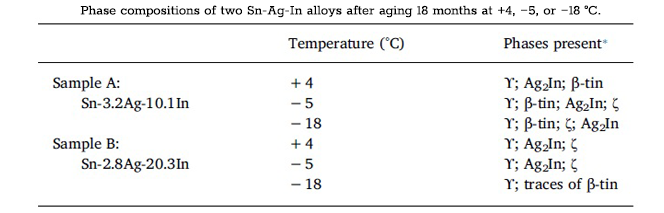
ζ is the solid solution between Ag3In and Ag4Sn.
γ =InSn4.
⁎ Phases are given in descending order of estimated quantities.
Influence of mechanical deformation
Mechanical treatments have been studied to understand the effect of various kinds of mechanical deformation on the formation of tin pest in lead-free solders [2,5,6,8,9,27]. Among the different treatments that have been studied are monotonic and cyclic strain, creep, and cold work or cold reduction. Tensile pre-strain has been shown to promote growth of tin pest in tin-coated steel, while earlier studies of tin pest formation in cold-worked samples have reported conflicting results, demonstrating a role for cold work in both promoting and in inhibiting the formation of tin pest [2].
Significant inconsistencies remain even among the most recent studies on the effect of cold work. In a study by Joo and Takemoto [28], the effect of cold reduction on incubation period and growth rate was investigated in cold-worked samples of Sn-0.8Cu. Samples were reduced by ratios of 20, 50, 80, and 90% with one group kept in the ascast condition (0% reduction) for comparison. Observations of “time until nucleation” and the subsequent rate of growth showed a direct correlation between %cold reduction and the length of the nucleation period (the following figure). The 90% reduced sample demonstrated the greatest susceptibility, with visible signs of tin pest appearing within 8 days of exposure. Growth rates between the 80 and 90% reduced samples were comparably fast, reaching nearly 100% transformation to α‑tin within 50 days. The as-cast comparator demonstrated the greatest resistance, remaining free of tin pest for up to 50 days. The subsequent growth in the sample took ~170 days to progress to completion. These results suggest that cold reduction increases tin pest susceptibility in lead-free alloys. It was suggested that the rapid rates of nucleation and growth were due to build up the internal strain energy from the mechanical treatment acting as an additional driving force, accelerating the β →α transformation.
The results by Joo and Takemoto [28] are supported by observations from Kariya et al. [7], where tin pest formed preferentially on the grip sections of tensile samples. The samples in the study were originally intended for tests of mechanical properties, as such; the heads of each sample were machined for gripping purposes. Formation of tin pest was observed to occur first and to a greater extent on the grip sections of every sample. Similar to the work of Joo and Takemoto, it was presumed that the work hardening of the grip sections built up residual stress in the material after machining and that this residual stress accelerated growth, providing an additional driving force for the transformation to gray tin.
Conflicting evidence is presented in the study by Peng [6], where cold-rolled samples of multiple alloys reduced to ~80% were observed to remain free of tin pest for periods of up to 5.5 years. Compared to incubation periods of other Sn-Cu alloys in the as-cast condition (~1 year) from Plumbridge, the 5.5+ years of tin pest resistance reported by Peng demonstrates a significant increase in the incubation period and suggests that cold-rolling promotes tin pest resistance.
The study by Peng [6] was published more recently than the work by Kariya et al. [7] and Joo and Takemoto [28]. The inconsistency between the results from Peng and the other two studies is addressed. Among the potential explanations offered for the inconsistencies were differences in sample preparation. In the study by Kariya et al. [7], samples did not receive the same proper cold reduction as the samples in Peng's study. Although it was noted by Kariya that the samples had received some work hardening from the machining of the specimen heads, the effect would have been minimal and localized; thus, samples were still classified as being kept in the as-cast condition. Peng suggested that by cold-rolling the samples, tin grains were elongated, the area of grain boundaries increased, and dislocations were generated; all of which contributed to the accumulation of residual stress in the sample matrix. It was suggested that the net effect was strengthening of the alloy, making the transformation from β →α tin more difficult.
The significantly shorter incubation period and accelerated growth observed in cold-worked samples by Joo and Takemoto were reported by Peng to potentially be the result of an additional aging treatment administered to the samples in the study by Peng. Prior to low-temperature exposure, samples in the study by Peng were aged for > 6 months at room temperature. As mentioned above, room temperature is a relatively high homologous temperature for these alloys where microstructural changes are well known to occur. Consumption of the deformation energy during the aging treatment by stress relaxation and microstructural changes such as coarsening was offered as one explanation for the inconsistency in results. The deformation energy was suggested in both the study by Kariya and the study by Joo and Takemoto to act as an additional driving force for the transformation. Consumption of this energy and thus, the absence of the additional driving force, could in theory account for the observed differences. Just like in earlier studies, the inconsistencies in the results mean the effect of work hardening is still unclear. The general trend among results, however, suggests that mechanical treatment most likely promotes formation of tin pest.
CALCE has published papers to have a comprehensive review of the tin pest phenomenon research and focuses on new experimental data regarding the formation of tin pest effects.
The data presented and analyzed here enable manufacturers to make the right decisions when choosing a tin-based alloy for low-temperature applications. Moreover, suggestions on how this information affects the lead-free industry and recommendations for future work to clarify and evaluate the occurrence of tin pest for electronic circuits are discussed.
Common arguments about the risks of using tin, especially whether tin alloys are acceptable for low-temperature applications and whether lead-free solders should be exempt from regulations, are also discussed.
The common assumptions are: (1) leadfree alloys can be safely used in low-temperature applications if solder paste joining technology is used, and (2) joints from solder paste benefit from both the presence of flux residues and tin oxide particles, which combined make the allotropic transformation extremely unlikely.
Please find the above-mentioned information in the Prof. Pecht's recent published papers, as listed in the following:
Many articles have been addressing the concerns with tin pest on the Sn-riched lead-free solders and are collected in this websitw. Some of them were focused on the tin pest trnasformation in Sn-based lead-free solders. Some of them were studying α- and β-Sn transformation between the bulk solder, solder paste, and tin powder. For example, Maio and Hunt also reported that the transformation of tin phase tended to occur in samples prepared from bulk solder than that from solder paste or tin powder. Their researches concluded that tin pest might not be a concern for newly developed lead-free alloys and can be appleid in the mission-critical electronics with more confidence. Moreover, applications and/or concerns on the components and equipment were also reported. On the other hand, studies on the muon mobility and kinetics between the α- and β-Sn were also performed to verify this transformation in the theoretical field. In the end, articles about the Exemption of lead in specidied areas are included here due to their low temperature applications.
Studies on the ß to α Sn transition in Sn-based lead-free solders
[7] Y. Kariya, N. Williams, C. Gagg, and W. Plumbridge, “
Tin pest in Sn-0.5 wt.% Cu lead-free solder,” The Journal of The Minerals, Metals & Materials Society (TMS), Vol. 53, No. 6, pp. 39-41, 2001.
[26] C. M. Gourlay, S. A. Beltakov, Z. L. Ma, and J. W. Xian, “
Nucleation and growth of tin in Pb-free solder joints,” The Journal of The Minerals, Metals & Materials Society (TMS), Vol. 67, No. 10, pp. 2383–2393, 2015.
[30] A. Skwarek, B. Illés, B. Horváth, A. Géczy, P. Zachariasz, and D. Bušek, “
Identification and characterization of ß→α-Sn transition in SnCu1 bulk alloy inoculated with InSb,” Journal of Materials Science: Materials in Electronics, Vol. 28, No. 21, pp. 16329-16335, 2017.
[31] Y. Du, C. Li, B. Huang, M. Tang, and C. Du, “
Research and prospect of binary high-temperature Pb-free solders”, Soldering & Surface Mount Technology, Vol. 27, No. 1, pp. 7-12, 2015.
[33] K. S. Kim, T. Imanishi, K. Suganuma, M. Ueshima, and R. Kato, “
Properties of low temperature Sn–Ag–Bi–In solder systems,” Microelectronics Reliability, Vol. 47, No. 7, pp. 1113-1119, 2007.
[34] I. De Ryck, E. Van Biezen, K. Leyssens, A. Adriaens, P. Storme, and F. Adams, “
Study of tin corrosion: the influence of alloying elements,” Journal of Cultural Heritage, Vol. 5, No. 2, pp.189-195, 2004.
Studies on α- and β-Sn transformation in tin materials
[22] K. Nogita, C. M. Gourlay, S. D. McDonald, S. Suenaga, J. Read, G. Zeng, and Q. F. Gu, “
XRD study of the kinetics of β ↔ α transformations in tin,” Philosophical Magazine, Vol. 93, No. 27, pp. 3627–3647, 2013.
[25] G. Zeng, S. D. McDonald, Q. F. Gu, K. Sweatman, and K. Nogita, “
Effect of element addition on the β →α transformation in tin,” Philosophical Magazine Letter, Vol. 94, No. 2, pp. 53–62, 2014.
Effects and evoluations of tin pest in the components and electronics
[1] N. D. Burns, “
A tin pest failure,” Journal of Failure Analysis and Prevention, Vol. 9, No. 5, pp. 461-465, 2009.
Applications on tin pest transformation
Studies on the muon mobility and kinetics between the α- and β-Sn
[39] O. Hartmann, I. R. Harris, D. Fort, P. J. C. King, and S. F. J. Cox, “
μSR studies of grey and white tin, α- and β-Sn,” Physica B: Condensed Matter, Vol. 404, Nos. 5-7, pp. 884-887, 2009.
Directives and Exemptions about the applications of lead
[4]
Directive 2011/65/EU (RoHS 2) came into force on 21 July 2011. Published in Official Journal L174, 1 July 2011 was transposed into national law by member states by 2 January 2013.
For questions or concerns regarding tin pests or CALCE's research into tin pest physics, composition, or microstructure, contact Professor Michael Pecht:
301-405-5323 | pecht@calce.umd.edu