Defect Description
Interfacial delamination of the interface between individual fibers and the organic resin matrix that provides pathway for conductive filament formation, this include measling and crazing by which the location of the delamination is specified at weave intersections. [1][2]
Defect Formation Process(s)
Possible causes for these defects include mechanical overstress due to poor drilling use of press fit pins and reflow soldering [1] [2]
|
List of Tests to Precipitate this Defect |
Failure Acceleration |
Likelihood to Precipitate this Defect (condition) |
Failure Mechanism(s) |
|
Temperature, Humidity, Bias |
• Humidity and high temperature increases moisture absorption by the laminate materials that accelerates filament growth [3] • Voltage gradient accelerates filament growth [3] |
✔ |
• Conductive Filament Formation |
|
Hot Step Stress |
• High temperature increases the moisture absorbed by the laminate materials given a threshold moisture content [3] |
✇ |
|
|
Thermal Shock |
• Thermal shock increases the chance of path formation due to interfacial degrdation between resin and fiber [3] |
✇ |
|
|
Combined Environment |
• Same as Thermal Shock |
✇ |
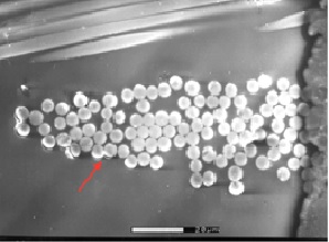 [4]
[4]
References
[1] IPC, Acceptability of Electronic Assemblies, IPC-A-610 Revision D, 2004
[2] Rogers K., Hillman C., Pecht M., and Nachbor S., "Conductive filament formation failure in a printed circuit board." Circuit World, vol. 25, no. 3, pp.6-8, 1999.
[3] Rudra B., Pecht,M., Jennings, D., “Assessing Time-to-Failure Due to Conductive Filament Formation in Multi-Layer Organic Laminates.” IEEE Transactions on Components, Packaging, and Manufacturing Techniques- Part B, vol. 17, no. 3, 1994.
Permission for pictures
[4] Rogers K., Hillman C., Pecht M., and Nachbor S., "Conductive filament formation failure in a printed circuit board." Circuit World, vol. 25, no. 3, pp.6-8, 1999.
Top