Explanation of the Stress Tests
Random Vibration (Vibration Step Stress)-Repetitive Shock Shaker
Stress Test Background
Apart from assessment of vibration reliability of electronic parts and systems, and for stress screening. Random vibration, in the form of Vibration Step Stress is one of the conventional stresses following the Cold, Hot Step Stress and Thermal Shock in HALT for the purpose of design margins improvement. Random vibration generated with repetitive shock (RS) shakers is a typical requirement in HALT, HASS standards and guidelines, while both RS shakers and electrodynamic (ED) shakers are typically accepted in ESS standards and guidelines.
Vibration from an RS shaker is one that originates from a repeated shock impulse excitation, typically created from pneumatic hammers impacting a vibration table to which test samples are attached. Compared to vibration from Electrodynamic (ED) shaker, RS shakers offer two main features that are beneficial for defect precipitation in electronics systems.
- Energy is focused on the higher frequency spectrum, which is more critical for testing smaller structures such as printed circuit boards and components.
- Simultaneous multi-axial vibration generates synergistic effects of all modes being excited and a more realistic vibration stress loading condition, which better approximates real world vibrations being experienced by products
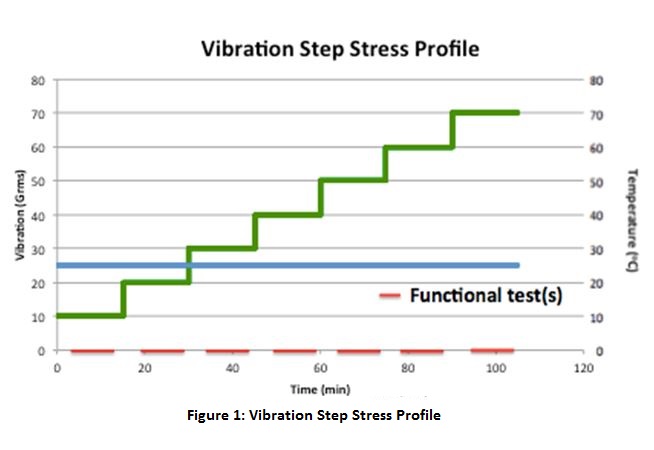
The stress profile shown in Figure 1 at the bottom resembles the test descriptions in IPC 9592A, IEST-RP-PR-003.1, and GMW 3172 for HALT. Apart from the ability in precipitating defects with the stress, detecting failures with functional tests, relationship between types of failures and discrete stress levels is also addressed in the profile design for proper corrective actions be made for the improvement in design margins.
Stress Profile Description
Typically start from 5 to 10 Grms, Then step down by fixed decrements to the maximum acceleration level with sufficient swell time at each step. Maximized functional test coverage should be optimized during testing.
Parameters Determination
Step Size
Based upon the accuracy required for failure point definition and the time available for testing. Reduce step size as failure point is reached is appropriate, which allows a fine definition without compromising test duration.
Dwell time
Should be determined based on the purpose of defect precipitation.
For design improvement purposes (HALT), a longer dwell time can be appropriate for more defects to be precipitated and corrected for field robustness of the product. It is suggested to be at least 10 minutes in both IPC 9592A and GMW 8287.
For screening purposes (HASS, ESS), also depend on the stress limits being decided, remaining life of the good population should be taken into account when deciding dwell time
Target stress level in this case, Maximum acceleration level
Should be determined based on the purpose of defect precipitation.
For design improvement purposes (HALT), stress levels to be high enough to precipitate defects that can cause failures below the desired stress limits or before the desired lifetime.
For screening purposes (HASS, ESS), target stress levels should be set lower to allow for sufficient remaining lifetime of the population with less critical defects remain in the products.
Standards with Stress Test Description
For Design Improvement Purpose
- IPC 9592A: Requirements for Power Conversion Devices for the Computer and Telecommunications Industries
- IEST RP PR 003.1: HALT and HASS
- GMW 8287: Highly Accelerated Life Testing (HALT) Highly Accelerated Stress Screening and Auditing
- MIL-HDBK 344A: Environmental Stress Screening (ESS) of Electronic Equipment
- MIL-HDBK 2164A: Environmental Stress Screening Process for Electronic Equipment
- IEST-RP-PR001.1: Management and Technical Guidelines for the ESS Process
- IEC-61163-1: Reliability Stress Screening
For Testing/ Acceptance Purpose
Typical Defects Precipitated by this Stress
|
Defect Location |
Typical Defects |
Failure Mechanism(s) |
|
Solder Joints |
Voids |
Mechanical Fatigue/ Overstress |
|
Cracks |
||
|
Cold Solder |
||
|
Insufficient Solder |
||
|
Corroded Solder |
||
|
Plated Through Holes (PTHs) |
Poor Hole Fill |
|
|
Glass Fiber Protrusion |
||
|
Irregular Plating |
||
|
Plating Voids |
||
|
Resin Smear |
||
|
Inner Plane Delamination |
||
|
Microvias |
Voids |
|
|
Poor Bonding of Pad/Via Interface |
||
|
Barrel/ Corner Cracks |
||
|
Metallizations |
Poor Hole Fill |
|
|
Glass Fiber Protrusion |
||
|
Irregular Plating |
||
|
Plating Voids |
||
|
Resin Smear |
||
|
Inner Plane Delamination |
||
|
Connectors |
Irregular Press Fit Pins |
|
|
Corroded Contacts |
||
|
Dust Accumulation |
||
|
Loosened Contacts |
||
|
Passive Parts/ Integrated Circuits |
Distorted Leads |
|
|
Poor Solderabiltiy of Leads |

References
Top