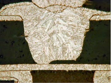
Defect Description
Bonding of the Pad/ Via interface is poor which can leads to crack initiation or delamination upon the exposure to environmental stresses.
Defect Formation Process(s)
Possible causes to this defect include:
i. Under-ablation
Resins are not sufficiently removed due to incorrect energy levels or poor trepanning techniques, creating a non-conductive barrier between the target pad and subsequent metallization [1]
ii. Contamination
Insufficient desmear causing the by-product form ablation process to trap
at the interface between pad/via plating boundaries, results in crack initiation at the interfaces [1-2]
iii. Insufficient surface preparation
The copper plating bath process involves various chemistries that prepare the surfaces for a strong chemical bond. For example, electroless copper on the target pad creates a strong bond to copper foil interface for a strong chemical bond, without such, foundation for the base of a microvia is not established [1].
|
List of Tests to Precipitate this Defect |
Failure Acceleration |
Likihood to Precipitate Defect (condition) |
Failure Mechanism(s) |
|
Thermal Shock |
• Thermal shock accelerates separation of copper-hole wall interface due to Coefficient of Thermal Expansion(CTE) mismatch |
✔ |
Thermal Fatigue/ Thermal Mechanical Overstress |
|
Random Vibration (RS/ED) |
• Random vibration can deteriorate of adhesion strength of the poorly bonded interface due to overstress or fatigue |
✔/✇ |
Mechanical Fatigue Mechanical Overstress |
|
Combined Environment |
• Combination of Thermal Shock and Random Vibration |
✔ |
Combination of Thermal Shock and Random Vibration |
|
Bend Test |
• Bending can separate poorly bonded interface due to mechanical overstress |
✇ (Defect at a location with significant strain due to bending) |
Mechanical Overstress |
References
[1] Ghaffarian R. “Reliability of PWB Microvias for High Density Package Assembly”, NASA Electronic Parts and Packaging Program (NEPP), 2006.
Top