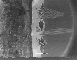
Defect Description
Presence of voids in and around the PTH wall that can cause stress concentrations for cracks to initiate upon the exposure to environmental stresses such as temperature cycling and vibration. Voids can be found around the glass bundles, in the area of the resin, at the inner layer interconnects [1].
Defect Formation Process(s)
There are many possible causes for this defect, they include
1. Rise in temperature of plating bath can create plating voids by reducing the gas solubility. This results in the nucleation of air bubbles within the plating bath [1-2].
2. In the electroless plating process, insufficient conditioner, acceleration, or catalysation will result in poor or no copper coverage over the glass fibers. A sluggish electroless bath will result in glass and resin voids [1-2].
|
List of Tests to Precipitate this Defect |
Failure Acceleration |
Likelihood to Precipitate this Defect (condition) |
Failure Mechanism(s) |
|
Thermal Shock |
• Cyclic thermal mechanical stress accelerates crack initiation or crack growth around the voids where local stress concentration is high • Thermal mechanical stress causes fracture of the copper plating at the protrusions where local stress concentration is high • Thermal mechanical stress can cause delamination if voids are present at the interface between copper plating and hole wall. |
✔ |
Thermal Fatigue Thermal Mechanical Overstress |
|
Random Vibration (RS/ED) |
• Random Vibration accelerates crack initiation or crack growth around the voids where local stress concentration is high • Vibration causes fracture of the copper plating around the voids where local stress concentration is high • Random Vibration accelerates separation of the poorly bonded interface if voids are present at the interface between copper plating and hole wall |
✔/✇ |
Mechanical Fatigue Mechanical Overstress |
|
Combined Environment |
• Combination of Thermal Shock and Random Vibration |
✔ |
Combination of Thermal Shock and Random Vibration |
|
Bend Test |
• Bending can cause fracture of the copper plating around the voids where local stress concentration is high • Bending can separate poorly bonded interface due to mechanical overstress if voids are present between copper plating and the hole wall |
✇ (Defect at a location with significant strain due to bending) |
Mechanical Overstress |
 [4]
[4]
References
[1] Tulkoff C., Hillman C., “Reliable plated through via design and fabrication.” DFR Solutions
[2] Minges, M. L Electronic Materials Handbook. Materials Park, OH: ASM International, 1989
[3] Tukloff C., Caswell G., Hillman C., “ Best Practices for Improving the PCB Supply Chain: Performing the Process Audit”, DFR Solutions
Permission for pictures
[4] Tulkoff C., Hillman C., “Reliable plated through via design and fabrication.” DFR Solutions
Top