Aris Christou1,2
1CALCE Research Center, Department of Mechanical Engineering
2Department of Materials Science, University of Maryland, College Park MD, USA
Abstract: Flexible display structures, powered by thin-film cells on the same substrate as the display pixels are reported. The display structure consists of arrays of thin-film transistors on polyethylene naphthalate. The nanoparticle technologies consisting of multiple layers of mixtures of activated carbon and ruthenium (IV) oxide for supercapacitors are reported. The mono-particulate layer process described here is a modified Langmuir-Blodgett trough. We report the processes for a spray-coated zinc nano-powder electrode used as a counter-electrode forming a galvanic cell of extremely high charge storage capacity (>40A-hr/cm2). Hydrated ruthenium oxide as a nano-powder (10-100nm) with a surface area that approaches tens of square meters per gram is layered with nano-powder activated carbon. Thin separating insulating layers are interposed between the RuO2 · xH2O and the counter-electrode. As the counter-electrode, thin films of zinc and aluminum, and powders of zinc for surface area enhancement have been applied. These cells are processed on flexible substrates in order to form a totally self-powered multi-pixel flexible display. Current-Voltage characteristics of thin-film transistors biased by the nanoparticle flexible batteries show fast power-on characteristics. Interconnects of both indium tin oxide and monolayers of graphene have been reported to show resistance to cyclical deformation.
I. Introduction
The field of flexible electronics is growing on many fronts and has achieved numerous applications within electronic systems. Various display needs require harsh environment, reliability, light weight as well are ideal for integration with a flexible power source or battery. Flexible displays are made possible by electro-optic devices integrated with an active matrix backplane which must have its own power system. Powered thin-film transistors in each display pixel must switch and power an electro-optic device. Other applications include integrated analog organic electronics, reconfigurable flexible antennas, as well as flexible pollutant detection for environmental applications. Micro autonomous sensor systems must also have the power system integrated with lightweight flexible electronics.
The present report is on the performance of an integrated power distribution system for flexible electronics in general and specifically for flexible displays. Our results are based on two substrates:
[1] Polyethylene naphthalate PEN from Dupont Teijin Films
[2] Stainless steel (Type 304 hard tension annealed)
Both substrates have a coefficient of linear expansion of approximately 18ppm/C – but each presents different mechanical stress issues in manufacturing. Stainless steel has layer adhesion and leakage problems while PEN appears to be stretching under stress from the thin films being deposited.
Amorphous Si:H thin-film transistors have been integrated via the source electrode with a thin film RuOx/Zn/Pb power cell. The present approach is to create a hydrated ruthenium oxide/ metal galvanic redox cell. In such a system, the electrolyte is charged by redox processes occurring at the RuO2/xH2O electrode.
The fabrication procedures for such flexible electronics are reported as well as an analysis of the amorphous silicon thin-film transistors. The electrical assessment of the integrated transistor-flexible battery is reported in the final section of the present paper. Finally, the mechanical stress limitations of power sources and thin-film electronics on flexible substrates are reported, since solution of such mechanical limitations is critical for future advances of a totally integrated, self- powered technology. A significant limitation of flexible electronics and flexible displays is the degradation induced by cyclical deformation of the entire display structure. The major limitation experienced in field operation has been the non-recoverable lineout effects, where a vertical line appears on the display. The line defects, once formed cannot be removed, and after continuous use, a significant number of line out defects appear which renders the display useless and is categorized as a failure. The lineouts are mainly vertical, but can also appear as a horizontal lineout and are independent of color since lineouts of the entire color spectrum can form.
Lineout defects are a manifestation of impedance buildup, and an increase in the interconnect resistance resulting in localized heat dissipation. Cyclical; deformation due to mechanical bending and also to cyclical powering leads to defect formation in the interconnect line and as a stress relief mechanism, the initiation of microcracks[1]. The state of the art material for these interconnect layers is Indium Tin Oxide (ITO) because of its combination of electrical and optical properties. [2], [3]. However, ITO is a brittle ionic material, forming micro-cracks during bending [4]–[7]. Graphene’s properties make it an ideal candidate to replace ITO as the interconnect material. Graphene’s mobility ranges from 15,000 up to 200,000 cm2/V·s [8]–[12]. Graphene also has a high optical transmittance with a value of 97.6% for a monolayer of graphene in comparison to ITO’s optical transmittance of 85% [2], [13]. Graphene has an Elastic modulus of ≈ 1 TPa and ultimate tensile strength of 120 GPa [14]. Bending stress studies on graphene have also shown that graphene can sustain more strain (5%) than ITO (1-2%) before reaching 10% change in resistance [15], [16]. However, there have been no reported results on the effect of cyclical deformation on both the electrical and optical properties of graphene. This information is critical for graphene on flexible substrates where numerous bending cycles will occur during the life of the product.
II. Experimental Approach
Fabrication Procedure
The present approach consists of fabricating the thin film transistors directly onto the Kapton or thin stainless steel flexible substrate and then connecting the power input interconnects to the flexible substrate using reflow soldering in order to provide bias to the source and drain of the MOSFETs. The fabrication of the integrated structure consisted of a flexible wafer with a pixel array and an area for test circuitry.
Figure 1a is a diagram of an individual pixel. The display allows each pixel to be addressed in the matrix by row and column drivers. The schematic diagram of an individual pixel circuit shows that it is composed of a thin film transistor, a capacitor connected between the transistor’s drain contact and ground, and the connection of the bottom electrode of pixel connected to the drain contact as well. Electro-optic material is then deposited on the bottom electrode, either electrophoretic or organic, and then a top transparent electrode is then deposited to complete the pixel[17-18]. The entire flexible wafer is shown in Figure 1b showing the TFTs, the display area, and the 64x64 pixel test structures.
|
Fig. 1A
|
Fig. 1B
|
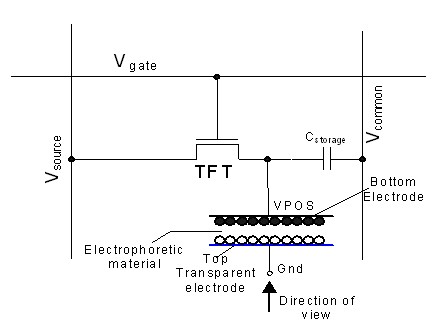
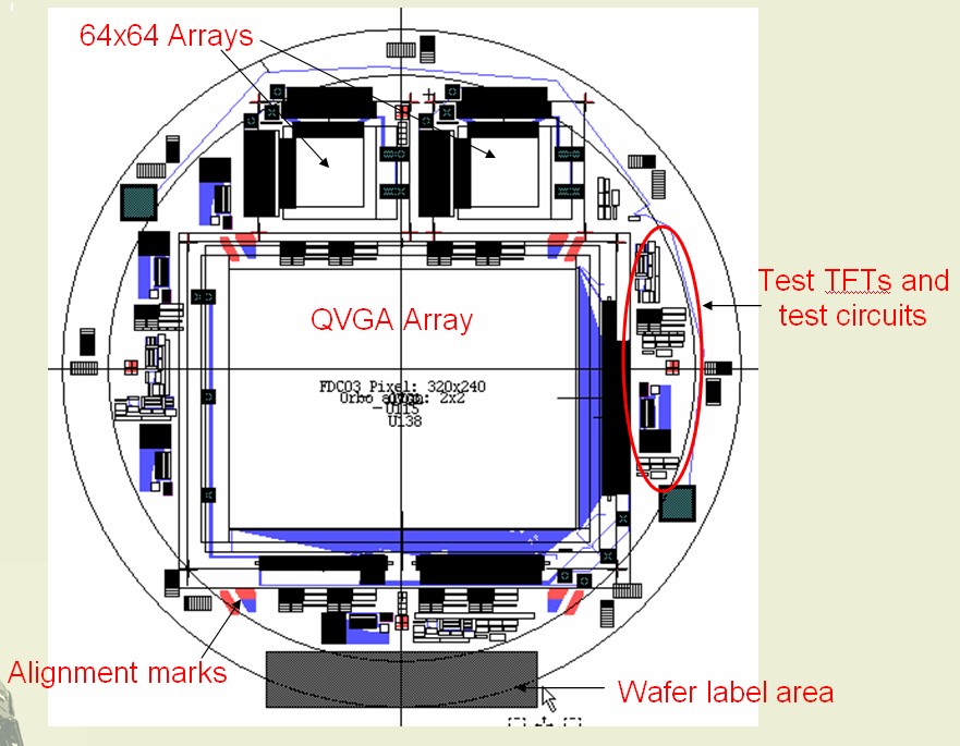
Fig.1. (a) A schematic of an individual pixel circuit, showing the thin film transistor and the capacitor, as well as the required connections. (b) The entire flexible wafer (3-inch diameter) is shown indicating the location of the test circuits and the display area
Signature of amorphous Silicon
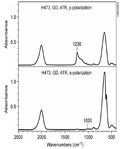
Fourier Transform Infrared (FTIR) Spectroscopy was used for determining the impurity concentration of the amorphous silicon being used. This will provide a signature of the material and give insight into the bending modes and bond vibrational modes. Figure 2 shows the spectra of a sample using polarized attenuated total reflection (ATR) measurements together with (FTIR) to investigate the vibrational spectra of a-SiHx/Si films 0.5-1.0 microns in thickness, showing characteristic bending modes at 2000 cm-1 as well as the vibrational spectra in the range of 600 cm-1. This signature shows the lack of hydride formation indicating typical FTIR characteristics for transistor active layers. Such signature analysis was used prior to fabrication in order to optimize transistor performance.
|
Fig. 2. Polarized FTIR-ATR spectra of a-SiHx/Si sample (Webb, 1999), [15]. |
Nano-Particle Based Battery
Electrochemical cells that can conform to a variety of electronic system packages, surface geometries as well as cells that can be embedded in flexible electronic systems are of tremendous technological importance [19]. Previous work has demonstrated that it is possible to make flexible cells with near-theoretical volumetric storage capacities. We present a flexible galvanic cell that can be optimized for volume manufacture and capable of integration with flexible electronic components. In addition, we describe a flexible cell whose attributes favor radio-frequency charging, as they are able to utilize low recharging voltages. Using the approach described in this paper, one can create “hybrids” of redox-cells and super-capacitors. These cells are based on chemicals with low toxicity and are thus environmentally benign. We show that the cells can achieve a specific capacity of over 2mA h/cm2.
The approach of the present work is to create a hydrated ruthenium oxide (RuO2 · xH2O) /metal galvanic redox cell (a battery). Previous investigations have reported that RuO2·xH2O has been used as a super-capacitor material due to its ability to generate high pseudo-capacitance. The electrolyte is charged by redox processes occurring at the RuO2·xH2O electrode. A dipole layer is formed by charge injection across the RuO2 · xH2O/electrode interface and the amount of charge transported is proportional to the change in electrode bias. The constant of proportionality is the pseudo-capacitance. This process has been previously reported [20-23].
Nanoparticles provide large surface-to-volume ratios and nano-particulate films can be made with exceptionally high surface area and the requisite porosity needed to form the electrolyte/electrode interface. The necessary nanoparticle coating technologies that can create “stackable” layers of nanostructures a single layer thick (100 nm) must be adapted to the present structure. Nano-particulate “hetero-structures” can thus be formed with well-controlled material proportions, just based on mean particulate diameter and size distributions. Hydrated ruthenium oxide as a nano-powder (10-100nm) was measured to have a surface area range of 10-20 square meters per gram. The Ruthenium oxide combined with activated carbon (AC), resulted in a decrease in surface resistance which was achieved at ten weight percent Ruthenium. The resulting compound was patterned using standard silk-screening techniques, which is not part of the present investigation. Thin separating insulating layers (0.5-micron thickness) was interposed between the RuO2 · xH2O and the counter-electrode. As the counter-electrode, we report the use of thin films of zinc and aluminum and powders of zinc for surface area enhancement.
This process is distinct from that of the electrochemical double-layer cell. In the present investigation, the electrode bias charge forms an image in the electrolyte and no mobile charge crosses the boundary. The performance of the super-capacitor is an indirect demonstration that the reduction of the RuO2·xH2O material was achieved.
As such, a redox couple was formed with a metal that can be oxidized (such as the zinc or aluminum anode) and a battery structure was achieved. As such, this investigation is the first report on the use of this material system as a redox cell. The relatively high internal resistance limits its application in large cell capacity systems but is ideal for microelectronic applications. For low power electronics, however, small amounts of current must be supplied over long periods of time. This offsets the internal dissipation of the cell. In addition, as we shall show, RuO2 · xH2O redox systems initially exhibit low internal resistance, enabling large amounts of “burst” power. In any event, it is clear that hybrid combinations of RuO2 · xH2O//metal and RuO2 · xH2O//RuO2 · xH2O electrode combinations can be made in which the first combination serves as a battery and the second as a super-capacitor, as described above.
There are a number of other potential advantages of the RuO2 · xH2O cell. Hydrated ruthenium oxide exists in a multiplicity of oxidation states and as the RuO2·xH2O/metal cell discharges, all of these oxidation states may be activated, leading to a “graceful” rather than a discontinuous drop in source potential. In the past, such a graceful discharge was viewed as undesirable for a battery. With the advent of ultralow-power, low-volume integrated circuit voltage regulators, this is no longer the case. All of these approaches yield viable electrochemical cells.
The implemented cells consist of an electrolyte composed of a weak acid and ethylene glycol that is close to neutral pH to prevent the rapid dissolution of the electrode materials or package sealing materials while favoring the needed redox reactions. In fact, the actual working pH is 5, which enables the reaction chemistry to proceed as close to equilibrium as possible to allow electrically driven reversibility (re-charging). The system of materials and the packaging approach used are targeted to yield a cell with a small weight, small volume, and high mechanical flexibility. Integration with thin-film transistors on a flexible polymer substrate has been achieved by attaching the battery via Van der Waals forces onto the common substrate.
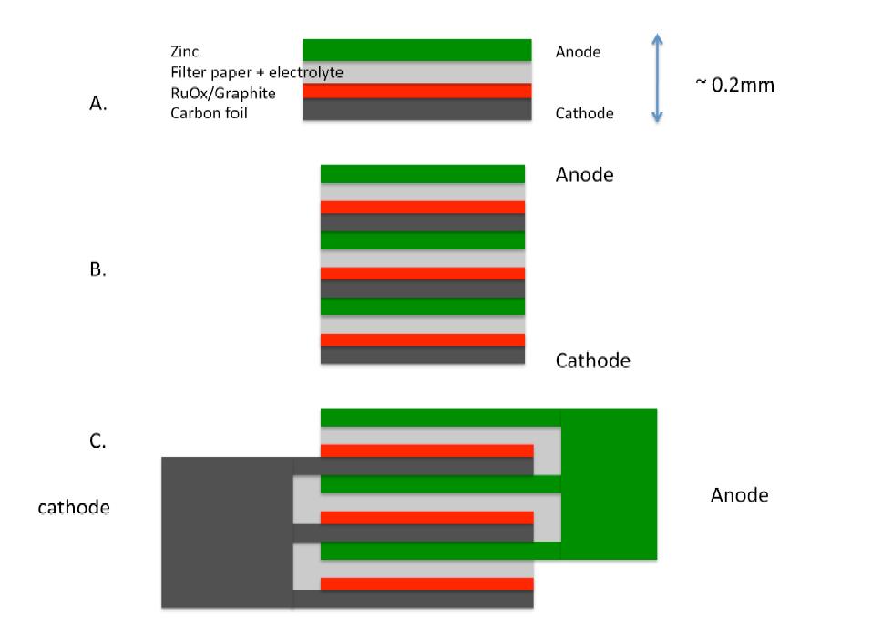
Displayed in Figure 3 is the physical cross-section of the fabricated flexible battery which was used to power the amorphous silicon thin-film transistors on a flexible substrate. In the schematic, the zinc layer is the anode, while the carbon-based foil is the cathode. These alternating layers may be stacked forming a multilayer integrated cell. Interconnects may be interdigitated resulting in a single contact point for either the anode or the cathode.
Again it must be emphasized that both galvanic cells and super-capacitors can be fabricated in the same process flow. A hetero-structure of two compounded ruthenium oxide electrodes (or a non-oxidizing electrode) forms a capacitor. Compounded ruthenium oxide electrodes on the surface of an oxidizing metal anode will form a battery. In all cases, the hybrid structure can be made thin and flexible. We now review the electrical behavior of the cells, as well as their capability for providing a bias voltage to thin-film transistors on flexible substrates.
|
|
Interconnects for Individual Pixels and Thin-Film Transistors
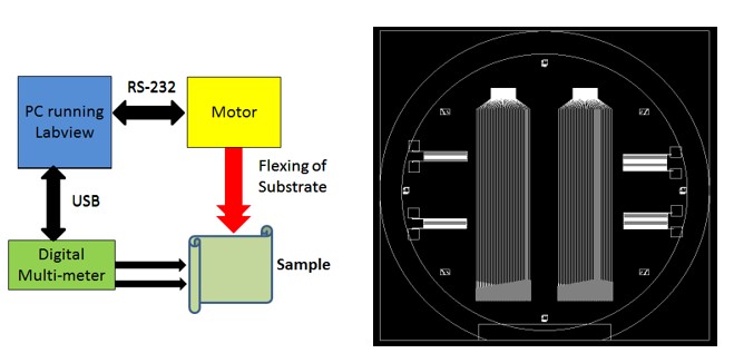
The cyclical deformation was accomplished by wrapping the flexible substrate structure around a cylindrical apparatus as reported previously [16]. The apparatus is then able to bend the sample to the desired radius of curvature, where the radius of curvature was directly correlated to the hoop stress exerted on the sample under test. The test apparatus was remotely controlled through an embedded microprocessor, while the radius of curvature can be varied by using a preselected set of cylinders. The bending stress then modifies the conducting properties of the interconnects and through finite element simulation the percent resistance change was correlated with the sample’s stress amplitude. Once the sample has been bent, resistance measurements are automatically measured using a digital multi-meter are taken and this process is repeated generating multiple cycles. An illustration of the test setup is shown below in Figure 4:
|
Fig. 4: Experimental setup based off cyclic mandrel method used for all fatigue testing of graphene, from ref 16. The interdigitated interconnect pattern is shown. |
Two types of interconnect test structures were fabricated and tested. For consistency, the layer test structures were used, with the ITO thickness maintained at 100 nm, and the three monolayer graphene samples were approximately 1-2 nm in thickness. One monolayer of graphene was measured to have a thickness of 0.33-0.35 nm. The geometric configuration was meandering interconnect lines (as shown in Figure 4) deposited on a 50 mm x 50 mm square substrate of Si3N4/PEN substrate. The substrate thickness was approximately 126 m of thickness and consisted of 1.0 m of Si3N4 deposited on 125 mm thick PEN polymeric substrate. The Si3N4 layer was deposited via Plasma Enhanced Chemical Vapor Deposition (PECVD) at 180°C. The temperature was kept below this level in order to ensure that the polymer did not degrade due to excessive heating. The ITO was deposited by DC sputtering at substrate temperatures below 100 C. The graphene films were obtained by a floating technique that consisted of graphene growth on a copper substrate and then transferring the graphene to the substrate of interest by floating the films in water initially.
III. Experimental Results
The RuO2· xH2O cells are capable of performing routine electronic system power sourcing operations, such as the flexible cell lighting based on LEDs, as well as providing a bias voltage to drive transistors for flexible displays. The capability for challenging source requirements such as power for integrated circuits is also achievable. Perfect IV characteristics for enhancement mode transistors have been obtained, as well as for transistors configured as an inverter chain. The surface geometry (15-micron gate widths) and typical current-voltage (IV) characteristics of these transistors are shown in Figure 5. These transistors were within a test wafer on a flexible pen substrate which was processed as part of our flexible display development project. These characteristics are indicative of excellent transistor action, showing a low series resistance and well behaved drain current versus drain voltage saturation.
Electrical Assessment of Power Cell Performance
Perhaps the most interesting aspect of the RuO2· xH2O cells is their short-term discharge capacity. The source current remains high (10-15 capacity of 0.2 mA-h/cm2 over the ten minute period. The long term discharge behavior of the battery through a large load (as would be typical of operation in an ultra-low power system) was examined. Note that the current remains higher than 0.4 μA for over 110 days. The integration to 110 days yields a 2.32 mA-h/cm2 specific storage capacity. When extrapolated to 150 days, this results in a specific storage capacity of 2.43 mW-h/cm2.
|
(a) |
(b) |
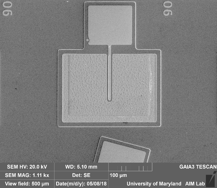
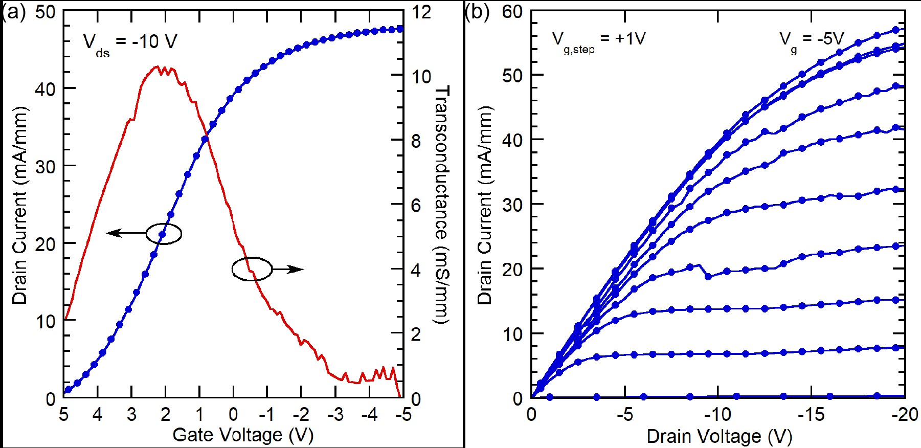
Fig. 5. (a) A top view of a flexible electronics thin-film drive single gate transistor. The substrate is stainless steel and the active material is amorphous silicon. (b) IV-characteristics of the nMOS transistor.
The discharge plots of a RuO2· xH2O/Zn cell for various loads are shown in Figure 6, showing traces taken over a 4-hour time interval. These results were obtained on single sheets of a flexible power cell with a 16 cm2 active area.
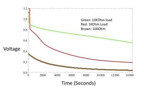 |
Fig. 6. Voltage versus time discharge plots for different loads.
The energy delivered for the zinc cell in a 24 h period corresponded to a power source of 0.7 mW/cm2. For a 10 K load, the voltage reduced linearly over time from 0.9 V to 0.6 V. The 10 K load is about the load a source would see looking into the supply interconnects of a typical low-power integrated circuit. Similar discharge plots were obtained for the RuO2 · xH2O/Al cell. In this case, the energy delivered in 24 h corresponded to a power density 0.3 mW/cm2 (Figure 6). The RuO2 · xH2O system is suitable for extremely low charging voltages. When an aluminum counter-electrode is substituted for zinc, the requisite charge voltage reduces to 0.8 volts, as shown in Figure 7, where a discharge plot following a 2 hour charge at a constant 0.8 V for the RuO2 · xH2O/Al system is shown. The discharge voltage saturates to 0.2 volts after 80,000 seconds.
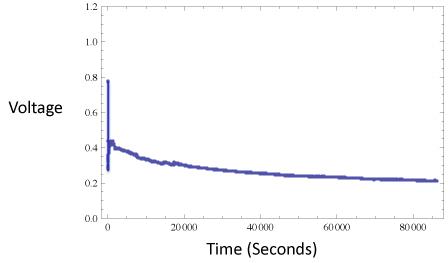 |
Fig.7. A 24-hour discharge plot for a RuO2 · xH2O/Al cell,(.5mW-h/cm2). Note that this 0.3 V voltage is fairly constant over the 24 h discharge.
Therefore, the results indicate that the RuO2 · xH2O-based redox cell can be configured as an electrochemical battery/super-capacitor hybrid resulting in an excellent performance. A composite structure made of cells of this battery type was able to supply over 30 mA for over 4.5 minutes into the bias supply interconnects of the input node in any type of distributed network, fully powering the node for that period of time. Furthermore, when the battery was taken off-line (terminals disconnected) for half an hour, the cell can fully power the node for an additional 4 minutes when re-connected.
In addition, the cells are environmentally benign and are easy to manufacture. No expensive processing or material handling equipment is required. While the ruthenium oxide is relatively expensive, it is but a percentage of the cathode, the rest being made up of activated carbon. We estimate the cost of fabrication of the cell to be less than $2 per square centimeter. Other advantages of this cell can be outlined as follows:
- Having an electrode of the large surface area allows for the passage of a relatively large current.
- The multiplicity of valence states allows for a “graceful” reduction in cell potential.
- This same multiplicity is likely to make the chemistry reversible.
So far, we have discussed electrical performance. However, we have determined that the main limitations to power integrated flexible electronics are strain effects induced by bending the substrate as well as strain from thermal expansion mismatch of materials. In the following section, we present a discussion of these mechanical effects on flexible electronics performance.
Interconnect Fatigue Results
The ITO test structures on Si3N4/PEN samples were mechanically cycle tested at three different stress amplitudes of 600, 500 and 400 MPa respectively. The fatigue tests were carried out at a frequency of 0.1 Hz until the failure criterion of 10% change in the normalized resistance was observed. The stress as a function of the number of cycles is shown below in Figure 8a for the first 50 cycles.
|
(a) |
(b) |
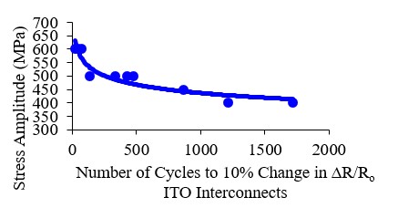
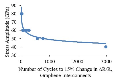
Fig. 8 a) Stress vs. Number of Cycles for ITO/Si3N4/PEN substrates tested at stress amplitudes of 600, 500, and 400 MPa respectively. b): Stress vs. Number of cycles for graphene/Si3N4/PEN substrates tested at stress amplitudes of 80, 60 and 40 GPa respectively.
Interconnects of Graphene on Si3N4/PEN substrates were tested at four different stress amplitudes of levels of 80, 60, 50 and 40 GPa respectively. Each of the samples was cyclically deformed at a frequency of 0.1 Hz until a 15% change in the normalized resistance was observed. The change in stress amplitude as a function of the number of cycles is shown below in Figure 8b for the first 50 cycles. The S-N curve shown in Figure 8b for Graphene shows the indication of the typical Coffin-Manson power-law relation with the number of cycles to failure. Graphene’s fatigue limit was found to be 40 GPa. The fatigue limit for ITO of 400 MPa was found to be significantly lower than that of graphene. The order of magnitude higher fatigue limit for graphene indicates that graphene is the more appropriate interconnect to withstand cyclical deformation effects and to prevent lineout defects in flexible displays.
IV. Discussion of Nano Mechanical Effects
Amorphous Si TFTs and Thin Film Battery
Since Organic TFTs do not currently match the performance of inorganic devices, amorphous silicon or nanocrystalline silicon has been used in the near term to fabricate the TFTs. It has been shown that the failure limit for a:Si TFTs is 0.5% in tension and up to 2% in compression, which is comparable to other inorganic materials [24].
Patterning the blanket a-Si layer into islands on the polymer substrate reduces the local strain on the islands, which is compensated in the polymer substrate between them [25]. A major challenge is an electrical interconnect to each TFT, but this may be a future approach for extending the mechanical limits in flexible electronics.
The mobility of TFTs is also affected by strain. It has been shown that for predictable, uniaxial strain, orienting the TFTs such that the channel current flows perpendicular to the applied stress reduces the drain current sensitivity by an order of magnitude relative to the parallel orientation [26]. The voltage output of the battery is expected to decrease due to strain effects from the substrate. A decrease in bias voltage may not turn on one of the bias transistors, resulting in dark line defects in a typical display. We expect therefore significant degradation in performance due to strain effects in flexible displays and in flexible electronics in general.
Metal Conductors
Unlike oxide materials, metal films do not experience brittle failure modes. Instead, metal films fail by localized deformation. The failure mode is initiated by the formation of a neck that becomes elongated and eventually leads to a rupture. The two most critical parameters that determine the rupture strain are (1) the modulus of the substrate and (2) the film adhesion. At 3% strain, an Au film on a low modulus silicone substrate shall start to fail. This figure is comparable to a freestanding film. Also, it has been noted that the substrate does not confine the elongation of the neck. If the substrate has a higher modulus, then deformation is more uniform and films can survive strains of greater than 10% - with the condition that the film and substrate have good adhesion.
Interlayer Effects
Once a failure occurs in a thin film, stress is relaxed locally and transferred to adjacent layers [27]. This means that while a device layer may withstand a uniform stress when tested alone, the same layer in a multilayer device may fail because of a failure in another layer of the stack. This effect is shown schematically in Figure 9. The implication is that, for example, while a single crack may not be catastrophic for an interconnect layer (such as Indium Tin Oxide layer, ITO), it may result in premature failure in a neighboring TFT that does result in catastrophic failure.
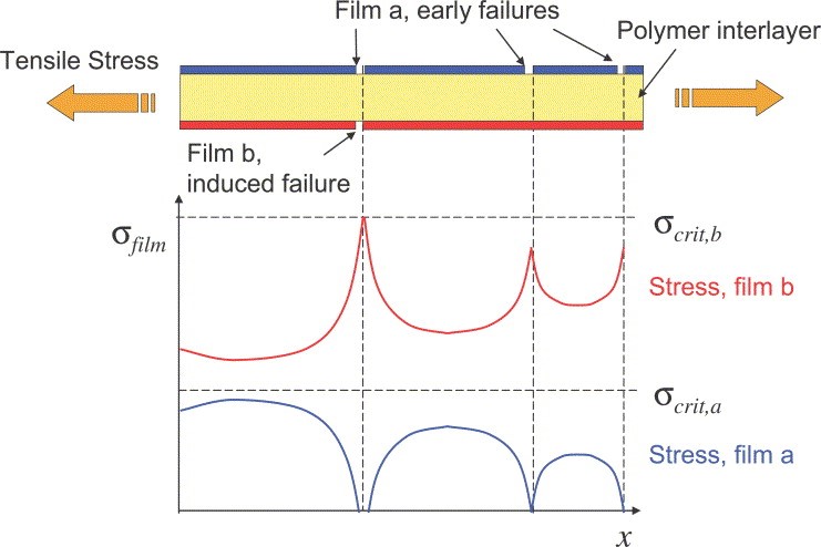 |
Fig.9. Layer interactions in thin films
Stress Reduction and Fatigue Limit
There are several strategies for reducing stress from device fabrication: modifying device materials, film thicknesses, geometry, deposition methods, deposition temperatures, and also film annealing. An alternate strategy to reduce mechanical stresses pertinent to the process integration of molybdenum/hydrogenated amorphous silicon TFTs was performed [28]. The previous approach was to minimize the intrinsic stress in the Mo layer through appropriate process conditions and film thicknesses – this resulted in narrow process latitude and a compromise in the performance of the resulting TFT. Alternatively, the stress was shown to be reduced by reducing the extrinsic stress by the underlying films through a different masking sequence in the fabrication. A 120°C process was developed that used a He-diluted 2.5% SiH4 + 97.5% (NH3+N2) mixture for the deposition of a-SiNx:H. This resulted in film densification and hydrogen release from SiH bonds – creating improved dielectric films that had smaller compressive stresses [29-31]. The further quantification of mechanical stress effects on flexible substrates is a topic under intense investigation and will be reported in a future publication. The existence of a fatigue limit in cyclically deformed ITO and graphene structures can not be explained at the present time but may be related to a graphene folding effect in monolayer films which may occur once a critical stress amplitude is reached.
Summary
In this paper, the advanced nanoparticle processing technologies that can create “stackable” layers of nanoparticles a single layer thick have been reported. Nano-particulate “hetero-structures” can thus be formed with well-controlled material dimensions and properties. As an example, it was shown that one can make layer mixtures of activated carbon and ruthenium (IV) oxide to create supercapacitors. The exact control and dispersion of controlled amounts of the oxide “enables” this process to be achieved with high yield. The mono-particulate layer process described here is a modified Langmuir-Blodgett trough. The particle dimensions were between 10-100 nm. No high-vacuum equipment or clean facility is required. Furthermore, it was shown how a spray-coated zinc powder electrode can be used as a counter-electrode forming a galvanic cell of extremely high charge storage capacity (>40A-hr/cm2). Both types of components can be made in the same process line, yielding a battery/super-capacitor hybrid. The resulting cells are flexible and thin (<0.3mm thick.).
The nanoparticle-based flexible batteries integrated with thin-film transistors as part of a flexible display is reported. In such a technology, a flexible flat panel display is enabled by an active matrix of devices and the flexible which replaces the conventional glass substrate (usually plastic or stainless steel). The most common type of active matrix is a thin-film transistor (TFT) array. The TFT array is also called a backplane, and display materials, such as electrophoretic displays (EPDs), liquid crystal displays (LCDs), and organic light-emitting diodes (OLEDs), are added on top. A required driving or bias voltage from the flexible, thin-film battery is applied at each pixel between the backplane and the common electrode which is the top electrode. We have successfully shown that the flexible power source is capable to bias the display drive transistors. The S-N fatigue behavior of Graphene on Si3N4/PEN and ITO on Si3N4/PEN has been determined. The S-N behavior of ITO does show a fatigue limit at 400 MPa while Graphene on flexible substrates shows a well-defined fatigue limit of 40 GPa. The high magnitude of the fatigue limit indicates that it should resist fatigue failures as interconnect for flexible electronics.
References
- L. Hrachowina et al, “Site Specific Growth of In-Situ Integration of Different Material Networks on a Single Chip,” ACS Sensors, 3, 3, 727-734 (2018).
- G. Domenech-Gil et al, “Localized and Integration of Different Nano-wire Materials for Electronic Nose Appl., Proc Eurosensors 2018, 2 (13) 457, Jan 2019.
- J. Deng et al, “Indium Tin Oxide on Saphire Microrods,” Sensors vol 20, 1289 (2020).
- Dinh-Phue Tran et al, “Conductive Characteristics of ITO Thin Films on Polymer Substrates Under Long-Term Static Deformation,” Coatings 8, 212 (2018).
- J.L.West, D.W. Lee, “Cracked ITO on Polyester Film Substrates for Electro-Optic Applications,” Appl Mechanics and Materials 526 15-20 (2014).
- M.F. Al-Kuhalli, J. of Materials Science: Materials in Electronics, vol 31 2729-2740 (2020).
- S. Seong, Y.C. Jung, T. Lee, I-S Park, J. Ahn, “Enhanced uniformity in electrical and optical properties of ITO,” Mater. Sci. Semicond. Proc. Vol 79, 14-19 (2018).
- H. Khachatryan, D-J. Kim et al, “Roll to Roll fabrication of ITO thin film for flexible optoelectronic applications, Mater. Sci. Semicond Proc 88, 51-56 (2018).
- V. Georgakilas, J.N. Tiwari, K.C. Kemp, J.A. Perman, Chem Rev 2016 116, 9, 5464-5519.
- Chui Chung, Y-K Kim, D. Shin, “Biomedical Applications of Graphene and Graphene Oxide,” Acc. Che,. Res. 2013, vol46, 10, 2211-2224 (2013).
- E. P. Randviir, Dale Brownson, J. Metters, “The Fabrication, Characterization and Electrochemical Investigation of Screen Printed Graphene Electrodes,” Phys. Chem. Chem. Phys., 2014, 16, 4598-4611 (2014).
- A. King, B. Davies, “A New Raman Metric for Characterization of Graphene Oxide and its Derivatives, “ Sci Rep vol 6, 19491, Jan 2016.
- V. Mayilvelnathan et al, “Characterization and Thermophysical Properties of Graphene,” vol. 676, 94-103 (2019).
- S. Sunar, R. Joffe et al, “Ultra high molecular weight polyethylene/ graphene oxide Nanocomposites, Thermal, mechanical and Wettability Characteristics,” Composites Part B: Engineering, vol 78, 185-191 (2015).
- Z. Luo et al, “Structure-Property Relationships in Graphene Based Strain and Pressure Sensors, Sensors 2019, 19(5), 1250 (2019).
- G. Paradee, Tom Martin and A. Christou, “Ftaigue Properties of ITO and Graphene on Flexible Substrates,” IEEE Trans on Dev Mat Rel, 15(3): 423-428 Aug 2015.
- K. L. Lin and K. Jain, "Design and Fabrication of Stretchable Multilayer Self-Aligned Interconnects for Flexible Electronics and Large-Area Sensor Arrays Using Excimer Laser Photoablation," in IEEE Electron Device Letters, vol. 30, no. 1, pp. 14-17, Jan. 2009.
- W. Dang, et al, “Printable Stretchable Interconnects,”in Flex. Print. Electron. 2 013003, Mar 2017.
- J. ur Rehman and M. H. Chowdhury, "Interconnects for Flexible and Printed Electronic Applications," 2019 IEEE International Conference on Flexible and Printable Sensors and Systems (FLEPS), Glasgow, United Kingdom, 2019, pp. 1-2.
- Jong-Hyun Ahn and Jung-Ho Je, “Stretchable electronics: materials, architectures and integrations”, Journal of Physics D: Applied Physics, Volume 45, Number 10, pp. 1-10, Feb 2012.
- C.F. Holmes and B.B. Owens, “Batteries for Implantable Biomedical Applications,” Wiley Encyclopedia of Biomedical Engineering, J. Wiley & Sons, New York City, NYC(2006).
- G. Nagasubramanian, D.H. Doughty, “Electrical Characterization of All-Solid-State Thin Film Batteries”, J.Power Sources 136, 395(2004).
- T. Suga, H. Konishi and H. Nishide, “Photocrosslinked Nitroxide Polymer Cathode-Active Materials for Application in an Organic-Based Paper Battery,” Chem. Comm.(Royal Society of Chemistry),1730(2007).
- L. Fragomeni, et al, "CMOS fully integrated 2.5GHz active RFID tag with on-chip antenna," Melecon 2010 - 2010 15th IEEE Mediterranean Electrotechnical Conference, Valletta, 2010, pp. 922-926 (2010).
- D. N. Wright et al., "Bending machine for testing reliability of flexible electronics," IMAPS Nordic Conference on Microelectronics Packaging (NordPac), Gothenburg, 2017, pp. 47-52 (2017).
- C. Zhang, H. S. Yang and M. S. Bakir, "Mechanically flexible interconnects with highly scalable pitch and large stand-off height for silicon interposer tile and bridge interconnection," 2014 IEEE 64th Electronic Components and Technology Conference (ECTC), Orlando, FL, pp. 13-19 (2014).
- Hao Liu et al, “Systematic Study on the Mechanical and Electric Behaviors of the nonbuckling interconnect Design of Stretchable Electronics,” in SCIENCE CHINA Physics, Mechanics & Astronomy, Volume 61, Issue 11: 114611(2018).
- J. Lewis, et al., Bend Testing of OLED devices on Polymer Substrates. Presented at Am. Vac. Soc., 52nd Int. Tech. Symp., Boston, MA, (2005).
- Chaoqi Zhang et al, “Mechanically flexible interconnects (MFIs) with highly scalable pitch” Journal of Micromechanics and Microengineering, Volume 24, Number 5, 23-35 (2014).
- K. Lee, H. J. Kim, I. Kim and K. W. Paik, "Ultrasonic Anisotropic Conductive Films (ACFs) Bonding of Flexible Substrates on Organic Rigid Boards at Room Temperature," 2007 Proceedings 57th Electronic Components and Technology Conference, Reno, NV, pp. 480-486 (2007).
- Alfred Gill, “Porous pSiCOH Ultralow-k Dielectrics for Chip Interconnects Prepared by PECVD”, Annual Review of Materials Research 39:1, 49-69 (2009).
Top