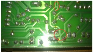
Defect Description
Surface traces that are exposed to sufficient conditions for electrochemical migration (ECM) process to initiate which can lead to shorting of two neighboring traces. The ECM process consists of path formation, electrodissolution, ion transport, electrodeposition and filament growth [1].
Defect Formation Process(s)
A typical migration path is created by the aggregation of water molecules combined with contaminant anions from flux residues to form an adsorbed layer of electrolyte capable of transporting metal ions between two neighboring traces [2].
|
List of Tests to Precipitate this Defect |
Failure Acceleration |
Likihood to Precipitate Defect (condition) |
Failure Mechanism(s) |
|
Temperature, Humidity, Bias |
• Humidity and high temperature accelerates dendrite growth by electrochemical migration [2-4] • The increase in voltage gradient increase probability of dendrite formation [5] |
✔ |
Electrochemical migration |
|
Hot Step Stress |
• High temperature increases the propagation rate of dentrites given the presence of moisture [4-5] |
✇ (The presence of moisture) |
|
|
Thermal Shock |
• Same as Hot Step Stress |
✇ (Same as Hot Step Stress) |
|
|
Combined Environment |
• Same as Hot Step Stress |
✇ (Same as Hot Step Stress) |
 [6]
[6]
References
[1] Zhan S., Azarian M. H., and Pecht M., “Surface insulation resistance of conformally coated printed circuit boards processed with no-clean flux,” IEEE Transaction on Electronic Package Manufacturing. vol. 29, no. 3, pp. 217–223, 2000.
[2] Zhan S., Azarian M. H., Pecht M., “Reliability of Printed Circuit Boards Processed Using No-Clean Flux Technology in Temperature-Humidity-Bias Conditions” IEEE Transactions on Device and Materials Reliability, vol. 8, no. 2, 2008.
[3] P. Lall, M. Pecht, and E. Hakim, Influence of Temperature on Microelectronics and System Reliability: A Physics of Failure Approach, CRC Press, New York, 1997.
[4] 8. G. DiGiacomo, “Metal Migration (Ag, Cu, Pb) in Encapsulated Modules and Time to Fail Model as a Function of the Environment and Package Properties,” IEEE/ Proceedings of the IRPS, pp. 27 – 33. 1982.
[5] L. Zou and C. Hunt, “The Effect of Test Voltage, Test Pattern and Board Finish on Surface Insulation Resistance Measurements for Various Fluxes,” NPL Report CMMT(A) 222, September 1999.
Permission for pictures
[6]"PCB Failure Investigation", PCB Assembly,PCB Manufacturing,PCB design - OURPCB, 2017. [Online]. Available: https://www.ourpcb.com/pcb-failure.html. [Accessed: 26- Apr- 2017].
Top